Programmable multi-mode built-in self-test and self-repair structure for embedded memory arrays

a memory array and self-repair technology, applied in the direction of electronic circuit testing, static storage, measurement devices, etc., can solve the problems of increased cost and complexity, many types of complex cell-interaction faults are frequently occurring, and the probability of defects inside these extremely compact on-board data storage subsystems is high, so as to achieve outstanding flexibility of the bisr architecture and speed up the bisr procedure

Active Publication Date: 2007-10-16
STMICROELECTRONICS SRL
View PDF11 Cites 41 Cited by
  • Summary
  • Abstract
  • Description
  • Claims
  • Application Information

AI Technical Summary

Benefits of technology

[0014]It is an object of the present invention to provide a more efficient and less cumbersome Built-In Self-Repair (BISR) circuitry for embedded RAMs in a device including also at least one nonvolatile memory array.
[0015]The complexity and burden of built-in self-repair (BISR) circuitry for distinct embedded RAMs of different sizes may be minimized according to the present invention by utilizing a single BIST structure for any number of distinct embedded memory arrays of different types and sizes.
[0017]The speed of the BISR procedure during mass production (Industrial mode), besides from benefiting from the possibility of carrying out a check of effectiveness of the substitution of a failed physical address with a redundancy structure without yet having written the new redundancy address in the nonvolatile memory array, is further enhanced by the outstanding flexibility of the BISR architecture allowed by modification of the programming of the selected test and repair flow, as well as by the coverage of logic location checking of the array. This eventually leads to consideration of pertinent information derived from an in-depth failure analysis that the BISR architecture allows during the prototyping phase.

Problems solved by technology

A direct consequence of the high level of integration of these complex devices is a high probability of defects inside these extremely compact on-board data storage subsystems.
In the newest fabrication technologies, with extremely reduced spacing, many types of complex cell-interaction faults are frequently occurring rather than and in addition to simple stuck-at faults.
In other words, if the device includes distinct RAM arrays of different sizes, a dedicated BIST module for each of them is normally required, implying an increased cost and complexity.
There are no BISR architectures capable of producing diagnostic information on the reasons why an embedded memory array having a certain inventory of redundancy structures are not repairable.
When a new device has entered the mass production stage, there can be sudden yield drops.
Of course, these investigations may be conducted on the devices through appropriate test programs using special external test set-ups, however these investigations are generally time consuming.

Method used


Image

  • Programmable multi-mode built-in self-test and self-repair structure for embedded memory arrays
  • Programmable multi-mode built-in self-test and self-repair structure for embedded memory arrays
  • Programmable multi-mode built-in self-test and self-repair structure for embedded memory arrays

Examples


Embodiment Construction

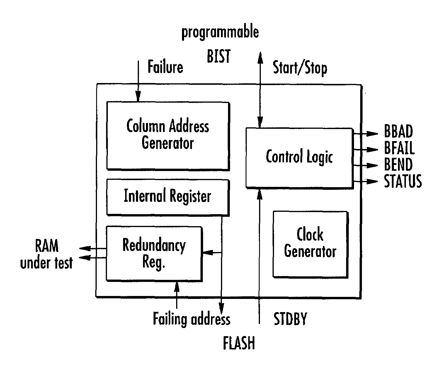
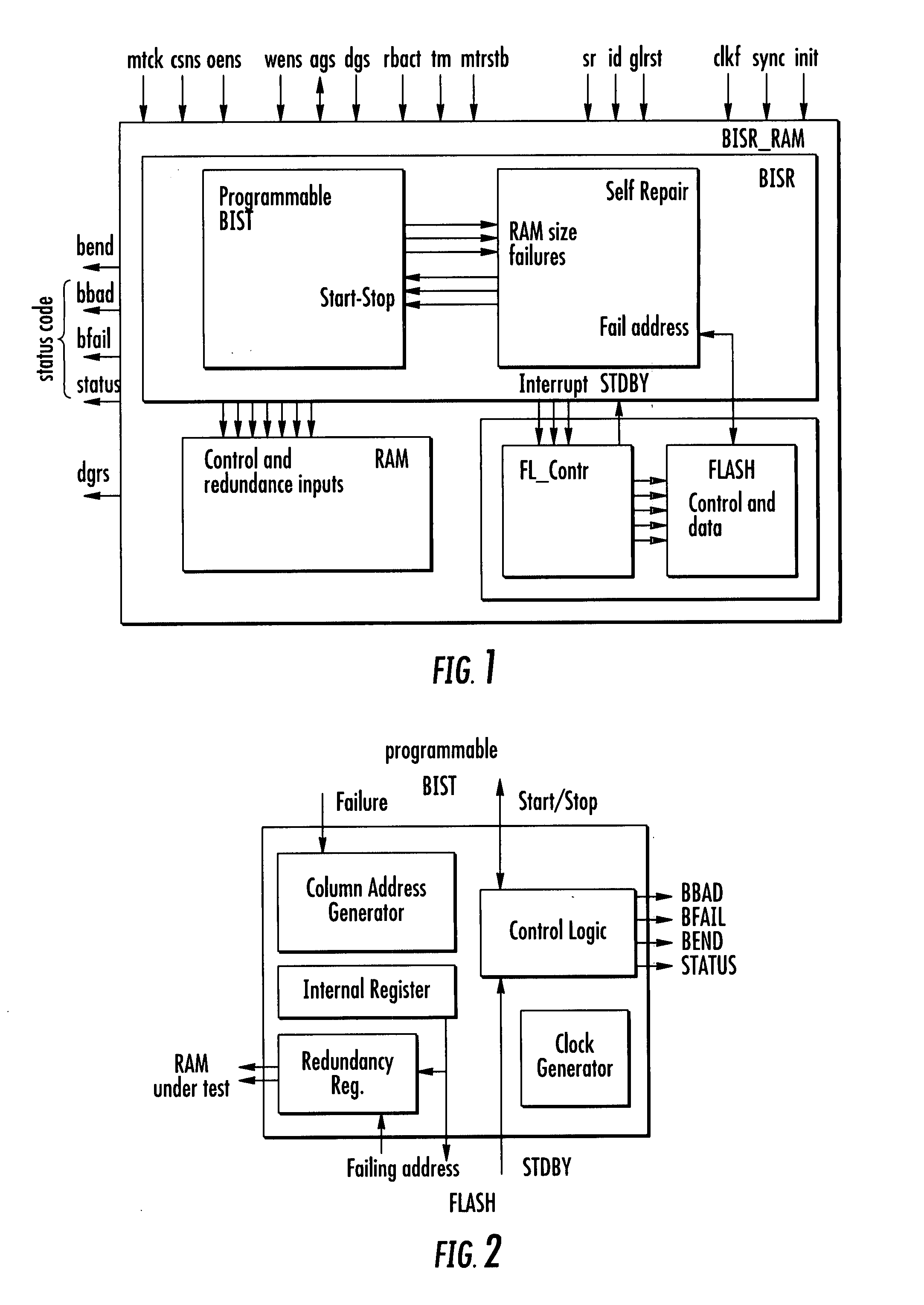
[0026]The architecture of the BISR machine of the present invention is shown in the functional block diagram of FIG. 1. The core of the BISR machine is the SELF-REPAIR block, that manages the enabling of the single programmable BIST that is used for testing the currently selected memory array RAM, elaborates the redundancy information and transfers them to the correct input ports of the RAM array being tested and repaired, and manages the communication with the nonvolatile memory FLASH that eventually stores the substituted addresses of the RAM.

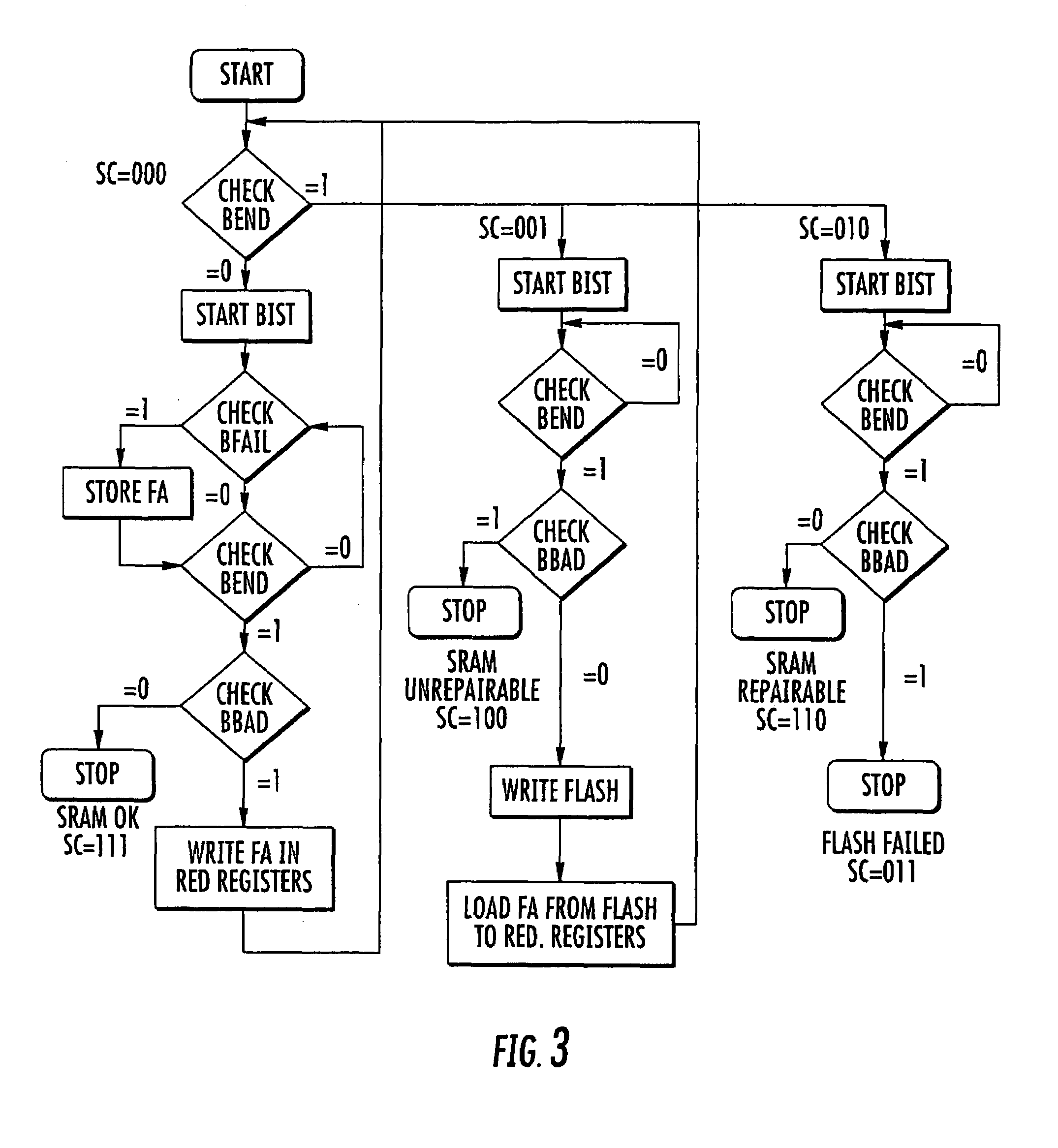
[0027]In the initial phase of a BISR session, the programmable BIST executes the test on the selected RAM by stimulating specific data pattern, related to a selected test algorithm. By reading the output data from the RAM and comparing them with the expected data, previously written in the memory under test and applied on the input memory ports by the programmable BIST, this allows the detection of any failing address and the identification o...


PUM


Abstract

A built-in self-test and self-repair structure (BISR) of memory arrays embedded in an integrated device includes at least a test block (BIST) programmable to execute on a respective memory array of the device any of a certain number of test algorithms, and a self-repair block that includes a column address generator processing the faulty address information for allocating redundant resources of the tested memory array. The BISR may further include a redundancy register on which final redundancy information is loaded at each power-on of the device and control logic for managing data transfer from external circuitry to the built-in self-test and self-repair structure (BISR) and vice versa. The BIST structure serves any number of embedded memory arrays even of different types and sizes.

Description

FIELD OF THE INVENTION[0001]The present invention relates, in general, to the testing and repair of embedded memories in system-on-chip or similar devices. More particularly, it relates to a built-in self repair architecture for testing and repairing embedded RAMs in a system comprising also nonvolatile memories.BACKGROUND OF THE INVENTION[0002]Embedded Random Access Memories (RAMs) have come to be one of the densest blocks in modern complex devices of which the so-called System-on-Chip (SoC) devices are significant examples. A direct consequence of the high level of integration of these complex devices is a high probability of defects inside these extremely compact on-board data storage subsystems. Redundant structures have therefore become a desired feature for embedded memories to achieve high production yields.[0003]Moreover, to enhance productivity by reducing the time required for testing embedded memory arrays of increasingly large capacities and for establishing the required...

Claims


Application Information

Patent Timeline
Patent Type & Authority Patents(United States)
IPC IPC(8): G11C29/00
CPCG11C29/16G11C29/4401G11C29/44G11C29/72
Inventor ZAPPA, RITASELVA, CAROLINARIMONDI, DANILOTORELLI, COSIMO
Owner STMICROELECTRONICS SRL
Why Eureka
Try Eureka