Method of fabricating non-volatile memory
a non-volatile memory and memory technology, applied in the field of memory fabrication, can solve the problems of increasing the level of integration of the sonos device with the split-gate cell structure, and the need for more memory space in the gate structure, and achieve the effect of increasing the level of integration of memory cells
- Summary
- Abstract
- Description
- Claims
- Application Information
AI Technical Summary
Benefits of technology
Problems solved by technology
Method used
Image


Examples
Embodiment Construction
[0036]Reference will now be made in detail to the present preferred embodiments of the invention, examples of which are illustrated in the accompanying drawings. Wherever possible, the same reference numbers are used in the drawings and the description to refer to the same or like parts.
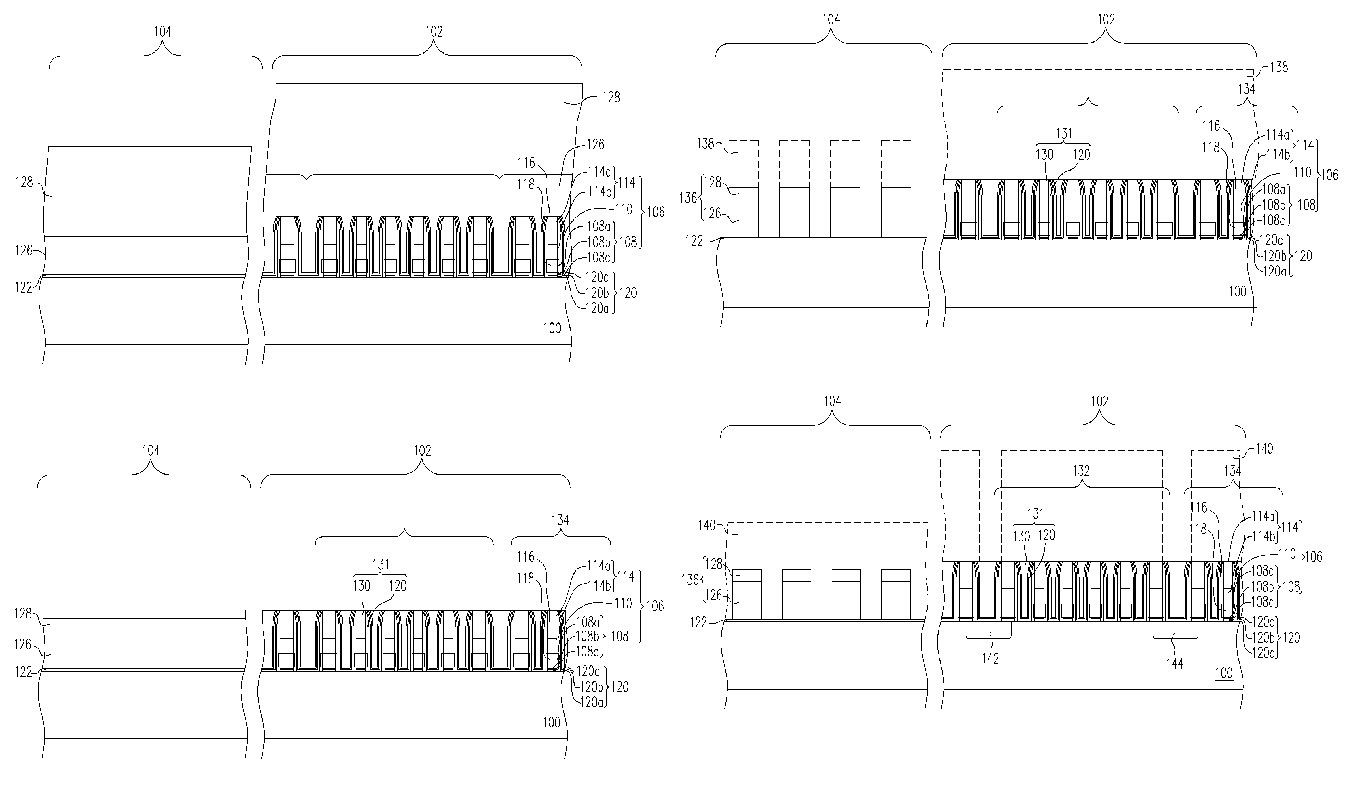
[0037]FIGS. 1A through 1G are schematic cross-sectional views showing the steps for fabricating a non-volatile memory according to one embodiment of the present invention. First, as shown in FIG. 1A, a substrate 100 such as a silicon substrate is provided. The substrate 100 can be divided at least into a memory cell region 102 and a peripheral circuit region 104. Then, a plurality of memory cells 106 is formed over the substrate 100 in the memory cell region 102. Each memory cell 106 includes a composite layer 108, a gate 110 and a cap layer 114. The method of forming the memory cells 106 includes sequentially forming a composite dielectric material layer, a conductive layer and an insulating materia...
PUM
 Abstract
Description
Claims
Application Information