Asynchronous-mode sync FIFO having automatic lookahead and deterministic tester operation

a synchronization and automatic lookahead technology, applied in the field of synchronization of data, can solve the problems of inaccurate data, data may not be received and sampled accurately in the receiving device, and the synchronization signal has limited precision in estimating the latency of the synchronizer

Active Publication Date: 2007-10-23
ADVANCED MICRO DEVICES INC
View PDF1 Cites 31 Cited by
  • Summary
  • Abstract
  • Description
  • Claims
  • Application Information

AI Technical Summary

Benefits of technology

[0013]There is a need for an arrangement that enables data to be read in a new clock domain at a minimum safe latency (i.e., the minimum latency without suffering metastability effects).
[0014]There is a need to be able to read data, having been obtained from across an asynchronous boundary, at the earliest possible safe time for minimum safe latency.
[0016]These and other needs are attained by the present invention, where data can be read in a new clock domain at a minimum safe latency based on identifying that a receive clock from a transmitting node is configured at operating only at prescribed available frequencies. A receive buffer circuit includes buffer control logic configured for reading a selected number of the buffer entries based on a detected number of receive clock edges within one local clock cycle. Valid data is identified based on the number of clock edges exceeding a selected threshold. A selected pointer offset is obtained from a lookahead table, specifying multiple pointer offsets for accommodating latency encountered at respective prescribed available frequencies, based on matching a determined frequency to one of the prescribed available frequencies. The selected pointer offset is added to a read pointer to offset the latency encountered from edge detection.
[0017]Hence, a more efficient implementation of a receive buffer circuit can be attained based on configuring the receive buffer circuit to operate only within the prescribed available frequencies. In addition, the selected threshold is selected from available thresholds based on the operational mode of the receive buffer circuit, enabling relaxed thresholds to be employed for deterministic testing.

Problems solved by technology

Note, however, that despite the common time base, the synchronization of data at the high data rates of 400 Mbs to 2.0 Gbs per wire is not trivial due to skew and phase locked loop (PLL) issues.
Hence, the data may not be received and sampled accurately in the receiving device because the receiver cannot simply rely on a fixed, simple ratio of clock frequencies as described above.
However, if the data is read too closely to the point where the data was latched, the data will be inaccurate (“bad data”) due to metastability effects.
However, the estimated latency calculated by the device of Hummel et al. assumes an arbitrary frequency for the transmit clock domain; hence, the synchronization signal has limited precision in estimating the latency of the synchronizer.
The tester, however, is only capable of checking for one specific pattern, and will consider all other behaviors failures, even if functionally the behavior is valid.
Hence, there is a concern that an integrated circuit may encounter “false failures” due to limited accepted patterns in chip test conditions.

Method used


Image

  • Asynchronous-mode sync FIFO having automatic lookahead and deterministic tester operation
  • Asynchronous-mode sync FIFO having automatic lookahead and deterministic tester operation
  • Asynchronous-mode sync FIFO having automatic lookahead and deterministic tester operation

Examples


Embodiment Construction

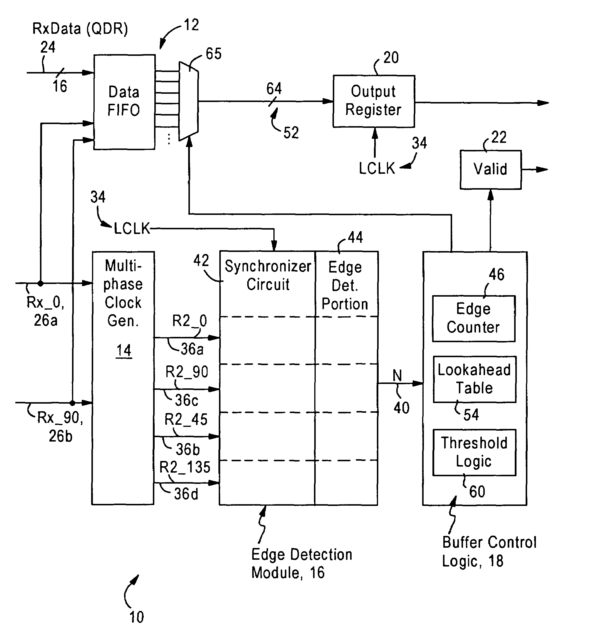
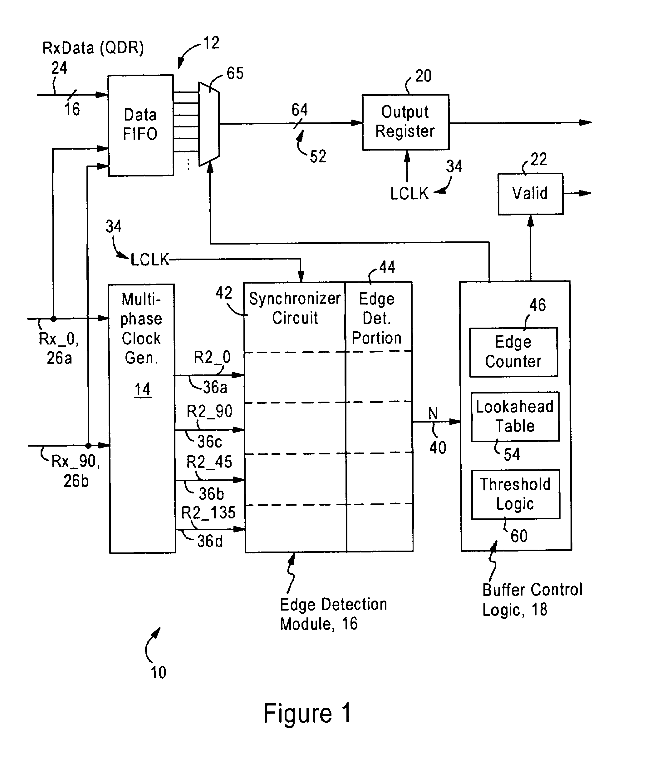
[0029]The disclosed embodiment is directed to an integrated circuit, for example a microprocessor or a device that interfaces with the microprocessor via a high-speed link such as a HyperTransport™ link, having a receive buffer circuit configured for outputting latched data signals based on synchronization between receive clocks generated by a transmitting clock domain, and a local clock generated within a receiver clock domain.

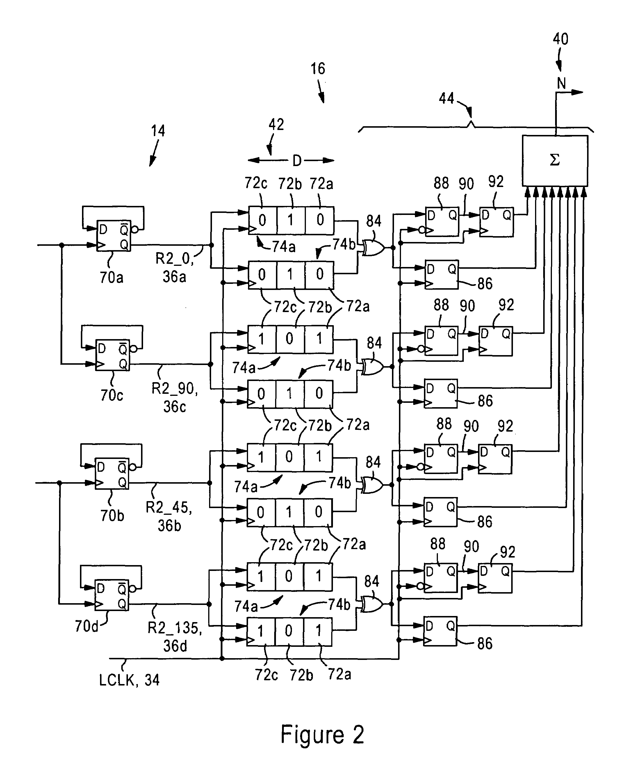
[0030]FIG. 1 is a diagram illustrating a receive buffer circuit 10 having a data buffer 12, a multi-phase clock generator 14, an edge detection module 16, and buffer control logic 18. The receive buffer circuit also includes an output register 20 configured for storing a 64-bit buffer entry output from the data buffer 12, and a valid bit register 22 configured for identifying the presence of valid data in the output register 20.

[0031]The First-In-First-Out (FIFO) buffer 12 is configured for receiving high speed data (RxDATA) via a parallel bus 24, for example...


PUM


Abstract

Precise estimation of latency is attained based on identifying that a receive clock is configured to operate only at prescribed available frequencies. A receive buffer circuit includes buffer control logic configured for reading a selected number of the buffer entries based on a detected number of receive clock edges within one local clock cycle. Valid data is identified based on the number of clock edges exceeding a selected threshold. A selected pointer offset is obtained from a lookahead table, specifying multiple pointer offsets for accommodating latency encountered at respective prescribed available frequencies, based on matching the determined frequency to one of the prescribed available frequencies. The selected pointer offset is added to a read pointer to offset the latency encountered from edge detection.

Description

BACKGROUND OF THE INVENTION[0001]1. Field of the Invention[0002]The present invention relates to synchronization of data, and more particularly, to a low latency method of synchronizing high-speed data to a local clock domain, where the high-speed data passes from one clock domain, across an asynchronous boundary, and into the local clock domain, enabling receipt and transfer of the high-speed data within an integrated circuit according to a local clock.[0003]2. Background Art[0004]Newer communications systems require advanced processing of high speed digital signals in order to accommodate precise timing requirements. For example, processor-based communications systems utilize high speed bus architectures, such as HyperTransport™ bus architectures, to transfer large groups of data at high data rates. For example, the HyperTransport™ Specification specifies data transfer between discrete components (e.g., between a microprocessor and a PCI bridge) in data groups (packets) of up to 6...

Claims


Application Information

Patent Timeline
Patent Type & Authority Patents(United States)
IPC IPC(8): G11C7/10G06F1/12H04L7/02
CPCG06F1/12H04L7/005H04L7/0338
Inventor OWEN, JONATHAN MERCERHUMMEL, MARK DOUGLAS
Owner ADVANCED MICRO DEVICES INC
Why Eureka
Try Eureka