Supercharge Your Innovation With Domain-Expert AI Agents!

Nonlithographic method of defining geometries for plasma and/or ion implantation treatments on a semiconductor wafer

a technology of plasma and/or ion implantation treatment and non-lithographic method, which is applied in the direction of photomechanical apparatus, coupling device connection, instruments, etc., can solve the problems of limited ability to reduce the physical dimensions of lithographically defined features on the wafer, extreme slowness, and the effect of reducing the productivity of the process

Inactive Publication Date: 2007-10-30
MICRON TECH INC
View PDF6 Cites 0 Cited by
  • Summary
  • Abstract
  • Description
  • Claims
  • Application Information

AI Technical Summary

Benefits of technology

The present invention provides a method for cost-effectively defining nanometric geometries for plasma and ion implantation treatments of semiconductor wafers. This is achieved by using a reusable mask or mask electrode that is more cost-effective than current methods. The mask is made by depositing a layer of refractory material on a mechanically self-sustaining substrate and then using RF power to transfer RF energy to the mask. The mask can be placed in contact or close proximity to the surface of the wafer, and the RF energy is capacitively transferred to the mask to enhance the desired plasma or ion trajectories. The invention offers higher productivity and cost savings compared to current methods.

Problems solved by technology

The ability of reducing the physical dimensions of the lithographically defined features on the wafer is limited by the technological ability of lithographically defining smaller and smaller details.
Although resolution is very high, the method is characterized by an extreme slowness (4-8 wafers / hour) and its productivity will probably remain relatively low.
Besides the cost of apparatus and infrastructure, advances in the technological limits of lithographic processings implies an ever increasing complexity of the processing operations that become more and more time consuming.

Method used


Image

  • Nonlithographic method of defining geometries for plasma and/or ion implantation treatments on a semiconductor wafer
  • Nonlithographic method of defining geometries for plasma and/or ion implantation treatments on a semiconductor wafer
  • Nonlithographic method of defining geometries for plasma and/or ion implantation treatments on a semiconductor wafer

Examples


Embodiment Construction

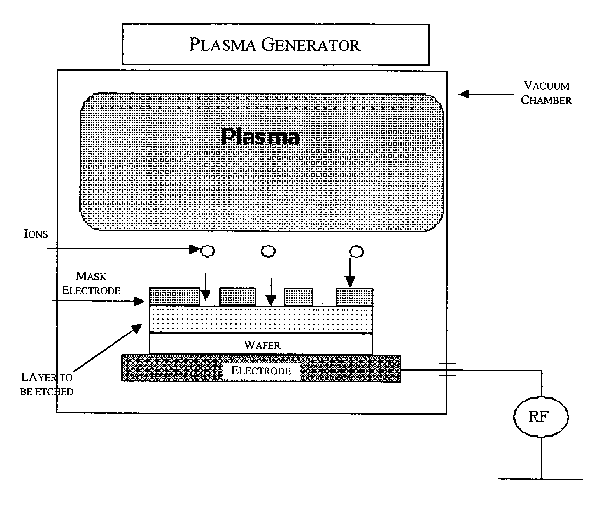
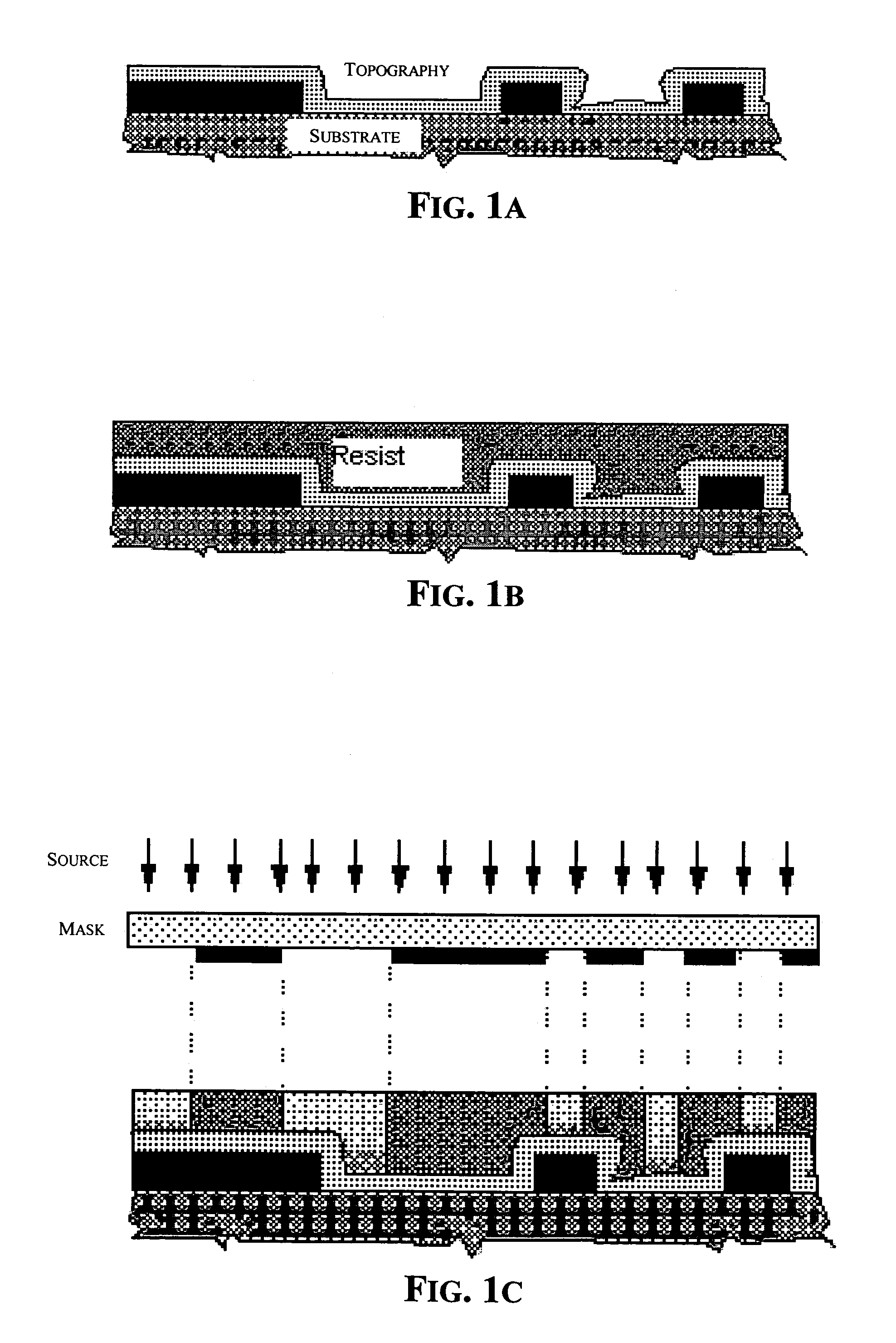
[0040]The main steps of a traditional plasma etching processing of a wafer are depicted in FIGS. 1a to if. FIG. 1a is a partial cross section of a generic wafer composed of a semiconductor substrate and onto which a certain feature has already been defined over its surface. A layer of a material (e.g., an isolation oxide layer) has been deposited on the semiconductor substrate and the certain features, and which is to be patterned.

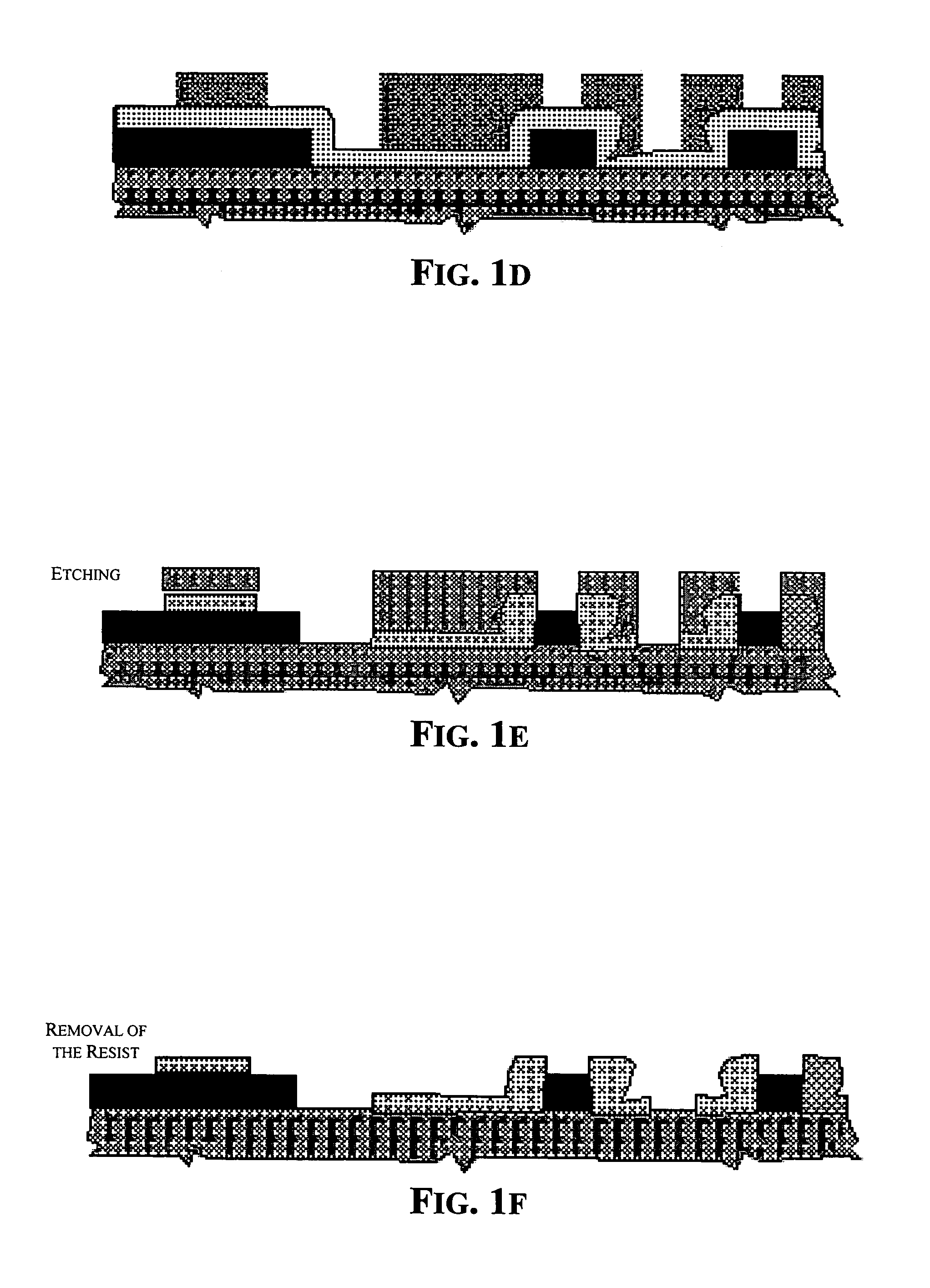
[0041]FIG. 1b shows a layer of photoresist deposited over the surface of the wafer. FIG. 1c depicts the phase of exposing the resist through a photolithographic mask, and producing a latent image of the photolithographic mask in the resist using a projection optical system. FIG. 1d shows the aspects of the resist mask formed on the wafer surface following the development of the exposed resist.

[0042]FIG. 1e shows the carrying out of a plasma etch through the resist mask openings of the underlying top layer of the wafer. FIG. 1f shows the new topography assu...


PUM

PropertyMeasurementUnit
thicknessaaaaaaaaaa
thicknessaaaaaaaaaa
distanceaaaaaaaaaa

Abstract

A method for defining geometries in a semiconductor wafer supported on a plate electrode in a processing chamber includes forming a reusable refractory coated laminar mask. The reusable refractory coated laminar mask is formed by defining the geometries in a laminar mask substrate, forming apertures through the laminar mask substrate, and forming a layer of refractory material over at least one surface of the laminar mask substrate. The reusable refractory coated laminar mask is positioned over the semiconductor wafer. Treating of the semiconductor wafer is performed through the apertures of the reusable refractory coated laminar mask. The treating may be plasma etching or ion etching.

Description

FIELD OF THE INVENTION[0001]The invention relates in general to semiconductor devices, and in particular, to fabrication techniques for defining geometries for plasma and / or ion implantation treatments of a semiconductor wafer supported on the surface of a plate electrode of a reactor.BACKGROUND OF THE INVENTION[0002]Advances in photolithographic techniques have been determinant in the success of the chip industry by allowing a continuous scaling down in the physical dimensions of the structures of integrated components, and consequently, in the cost of semiconductor devices.[0003]These results have been achieved by using radiation of smaller and smaller wavelengths (λ), and increasingly large numerical apertures (NA) of the optical system by implementing techniques based on phase contrast lithographic masks (PFM) and off-axis or annular illumination and use of high performance resist. The resolution of the optical system is proportional to the ratio (λ / NA).[0004]Basically, photolit...

Claims


Application Information

Patent Timeline
Patent Type & Authority Patents(United States)
IPC IPC(8): H01L21/302G03F1/20G03F7/00
CPCG03F7/0015G03F1/20H01J2237/31788H01J2237/0453
Inventor ALBA, SIMONEROMEO, CARMELO
Owner MICRON TECH INC
Features
  • R&D
  • Intellectual Property
  • Life Sciences
  • Materials
  • Tech Scout
  • Unparalleled Data Quality
  • Higher Quality Content
  • 60% Fewer Hallucinations
Learn More