Shift register and a display device using the same

a technology of display device and shift register, which is applied in the direction of digital storage, optics, instruments, etc., can solve the problems of complex fabrication process of a-si tft lcd, high fabrication cost, and complicated olb (outer lead bonding) process, and achieve the effect of stable operation

Inactive Publication Date: 2007-10-30
SAMSUNG DISPLAY CO LTD
View PDF30 Cites 95 Cited by
  • Summary
  • Abstract
  • Description
  • Claims
  • Application Information

AI Technical Summary

Benefits of technology

[0021]Accordingly, it is a first object of the present invention to provide a shift register making it possible to perform a stable operation regardless of the fluctuation in the threshold voltage of a-Si TFT LCD on a use of a long-term by maintaining an input node of the full-down means at a coupled status with the power voltage.
[0022]It is a second object of the present invention to provide an LCD capable of minimizing the number of external connection terminals on the LCD panel for the connection with an external circuit by using two clock signals.
[0049]Moreover, the second power voltage is above a threshold voltage capable of turning on the third transistor even when the first power voltage is applied to the gate terminal of the third transistor and less than the first power voltage. The external input control signal has a voltage level capable of turning off the transistor while the start signal is applied to the first stage and an output of a last shift register is generated, and turning on the transistor after the output of the last shift register is generated, thereby discharging the charge accumulated in the capacitor of the last shift register.

Problems solved by technology

Poly-Si TFT-LCD has advantages of lower power consumption, lower price compared with a-Si TFT-LCD but has a drawback in that its manufacturing process is complicated.
Thus, since multiple flexible PCBs should be assembled in a glass substrate, a fabrication process of a-Si TFT LCD, especially OLB (Outer Lead Bonding) process becomes complicated compared with that of poly-Si TFT LCD, whereby its fabrication costs becomes higher.

Method used


Image

  • Shift register and a display device using the same
  • Shift register and a display device using the same
  • Shift register and a display device using the same

Examples


embodiment 1

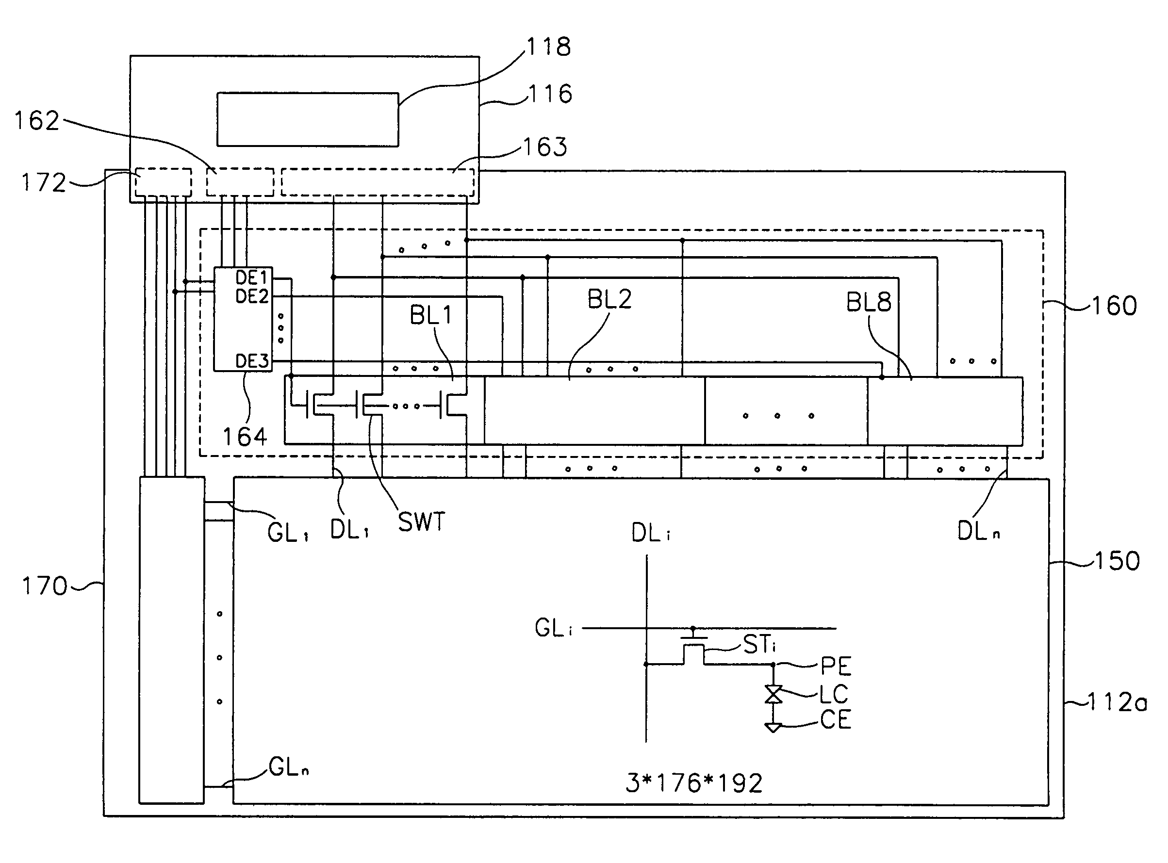
[0121]Hereinafter, there is described a concrete circuit constitution of each stage of the shift registers in the aforementioned data driving circuit and gate driving circuit with reference to FIG. 7.

[0122]Referring to FIG. 7, each stage of the shift registers 164 and 170 includes a pull-up section 180, a pull-down section 182, a pull-up driving section 184, a pull-down driving section 186, a floating preventing section 188 and a turn-on preventing section 190.

[0123]The pull-up section 180 includes a pull-up NMOS transistor NT1 of which drain is connected to a clock signal input terminal CK, gate is connected to a first node N1 and source is connected to an output terminal OUT.

[0124]The pull-down section 182 includes a pull-down NMOS transistor NT2 of which drain is connected to an output terminal OUT, gate is connected to a second node N2 and source is connected to a first power voltage VSS.

[0125]The pull-up driving section 184 includes a capacitor C and an NMOS transistor NT3 to N...

embodiment 2

[0147]FIG. 15 is a circuit diagram of each stage of the shift registers in the data driving circuit and the gate driving circuit.

[0148]Referring to FIG. 15, each stage of the shift registers 164 and 170 includes a pull-up section 190 a pull-down section 192, a pull-up driving section 194 and a pull-down driving section 196.

[0149]The pull-up section 190 includes a pull-up NMOS transistor NT11 whose drain is connected with a clock signal input terminal CK, gate is connected with a third node N3 and source is connected with an output terminal OUT.

[0150]The pull-down section 192 includes a pull-down NMOS transistor NT12 whose drain is connected with the output terminal OUT, gate is connected with a fourth node N4 and source is connected with a first power voltage VSS.

[0151]The pull-up driving section 194 includes a capacitor C and NMOS transistors NT13, NT14 and NT15. The capacitor C is connected between the third node N3 and the output terminal OUT. The transistor NT13 includes drain c...

embodiment 3

[0170]FIG. 20 is a circuit diagram of each stage in the shift register in accordance with a third embodiment of the present invention and FIG. 21 is a timing diagram for illustrating the driving waveform of the shift register of FIG. 20.

[0171]Referring to FIG. 20, each stage of the shift registers 170 in accordance with the third embodiment of the invention includes a pull-up section 190, a pull-down section 192, a pull-up driving section 194 and a pull-down driving section 196.

[0172]The pull-up section 190 includes a pull-up NMOS transistor M2 of which drain is connected to a clock signal input terminal CK, gate is connected to a fifth node N5 and source is connected to an output terminal GOUT.

[0173]The pull-down section 192 includes a pull-down NMOS transistor M3 of which drain is connected to the output terminal OUT, gate is connected to a sixth node N6 and source is connected to a first power voltage VSS.

[0174]The pull-up driving section 194 includes a capacitor C and NMOS trans...


PUM

PropertyMeasurementUnit
widthaaaaaaaaaa
hold timeaaaaaaaaaa
delay falling timeaaaaaaaaaa

Abstract

A shift register in which multiple stages are connected one after another to each other, the multiple stages having a first stage in which a start signal is coupled to an input terminal, the shift register sequentially outputting output signals of respective stages. The multiple stages have odd stages for receiving a first clock signal, and even stages for receiving a second clock signal having a phase opposite to the first clock signal. Each of the multiple stages has a pull-up section for providing a corresponding one of the first and second clock signals to an output terminal. A pull-up driving section is connected to an input node of the pull-up section. A pull-down section provides a first power voltage to the output terminal. A pull-down driving section is connected to an input node of the pull-down section.

Description

[0001]This is a continuation application of the U.S. patent application Ser. No. 10 / 068,892 filed on Feb. 11, 2002, which has now become U.S. Pat. No. 6,690,347.BACKGROUND OF THE INVENTION[0002]1. Field of the Invention[0003]The present invention relates to a shift register of a display device and a liquid crystal display (LCD) using the same, and more particularly, to a shift register generating a scanning signal for scanning gate lines in a gate line driving circuit of AMTFT-LCD (Active Matrix Thin Film Transistor Liquid Crystal Display) and for selecting a block of data lines in a data line block driving circuit.[0004]2. Description of the Related Art[0005]In these days, information processing devices have been rapidly developed in a trend with various architectures, functions and faster information processing speed. Information processed in these information processing devices has an electrical signal format. In order to visually confirm information processed in the information ...

Claims


Application Information

Patent Timeline
Patent Type & Authority Patents(United States)
IPC IPC(8): G09G3/36G02F1/133G09G3/20G11C19/00G11C19/18G11C19/28
CPCG09G3/3648G09G3/3666G09G3/3677G09G3/3688G11C19/28G11C19/184G09G2300/0408G09G2310/0218G09G2310/0286G09G2310/0297G09G2352/00G09G2300/0426G02F1/133
Inventor JEON, JINKIM, HYUNG-GUELMOON, SEUNG-HWAN
Owner SAMSUNG DISPLAY CO LTD
Why Eureka
Try Eureka