Method of isolation for acoustic resonator device

a resonator device and acoustic energy technology, applied in piezoelectric/electrostrictive transducers, device material selection, conductive pattern formation, etc., can solve the problems of reducing affecting the efficiency and performance of the device, and affecting the efficiency of the device, so as to prevent the growth of the device, reduce the amount of acoustic energy, and inhibit the effect of device efficiency and performan

Inactive Publication Date: 2007-11-20
BELL SEMICON LLC
View PDF67 Cites 16 Cited by
  • Summary
  • Abstract
  • Description
  • Claims
  • Application Information

AI Technical Summary

Benefits of technology

[0006]The present invention provides a method of isolating acoustic resonator devices formed from a piezoelectric material that is interposed between two conductors on a substrate. For example, a region of piezoelectric material surrounding or partially surrounding a device, between at least two devices may be removed, it may be prevented from growing in that region during fabrication of the devices, or it may have a crystal orientation within that region altered. Each of these techniques may reduce the amount of acoustic energy which propagates in a lateral direction away from the device. This loss of acoustic energy may inhibit device efficiency and performance, and could interfere with adjacent or adjoining devices and components.

Problems solved by technology

Each of these techniques may reduce the amount of acoustic energy which propagates in a lateral direction away from the device.
This loss of acoustic energy may inhibit device efficiency and performance, and could interfere with adjacent or adjoining devices and components.

Method used


Image

  • Method of isolation for acoustic resonator device
  • Method of isolation for acoustic resonator device
  • Method of isolation for acoustic resonator device

Examples


first embodiment

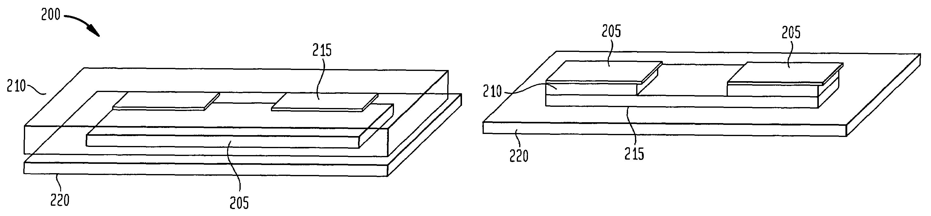
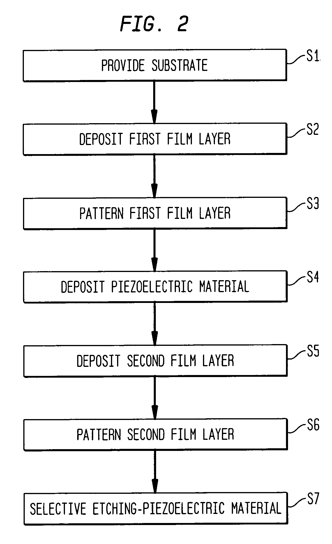
[0018]FIG. 2 illustrates the method of isolating an acoustic resonator device in accordance with the present application. Though there can be a myriad of thin film process steps involved in the batch fabrication of a TFR acoustic resonator device as there is in fabricating any modern integrated circuit, the vast majority of these processes involve repeated applications of three primary operations: deposition, lithography, and etching.

[0019]Referring to FIG. 2, initially a base support structure such as a substrate is provided (Step S1). In this case, the base structure is not integral to device operation; it primarily provides mechanical support. The base structure, hereinafter “substrate” may be a silicon wafer substrate, and preferably may include a plurality of alternating acoustic reflecting layers of acoustically mismatched materials such as SiO2 and AIN which are mounted on a solid substrate such as a silicon, quartz, or glass wafer. Further, the substrate may be a membrane wh...

third embodiment

[0033]The piezoelectric effect, and therefore the performance of the TFR, is thus strongly affected by the orientation of the piezoelectric crystals. The crystalline orientation, in turn, is highly sensitive to the surface upon which the material is grown. The third embodiment leverages this sensitivity to substrate surface structure by pre-patterning the substrate into regions where the material will grow with well-oriented crystalline structure and those where it will grow with poor orientation. In this embodiment, the crystal structure is “disrupted” in regions outside the discrete resonator structures, rendering those regions incapable of transducing waves, mechanically different than the oriented material such that an acoustic reflection will occur, and if disrupted or altered enough (such that for example crystal morphology is strongly affected) of even transmitting an acoustic wave.

[0034]Referring to FIG. 8, after obtaining the substrate (Step S21), a first metal film is depo...


PUM

PropertyMeasurementUnit
thickaaaaaaaaaa
thickaaaaaaaaaa
piezoelectricaaaaaaaaaa

Abstract

A method of isolating piezoelectric thin film acoustic resonator devices to prevent laterally propagating waves generated by the device from leaving the device and / or interfering with adjacent devices or systems. Specifically, this isolation technique involves the manipulation or isolation of the piezoelectric material layer between the acoustic resonator devices, in an effort to limit the amount of acoustic energy which propagates in a lateral direction away from the device. In one aspect, at least a portion of the piezoelectric material not involved in signal transmission by transduction between RF and acoustic energy is removed from the device. In another aspect, the growth a piezoelectric material is limited to certain regions during fabrication of the device. In a further aspect, the crystal orientation of the piezoelectric material is disrupted or altered during device fabrication so as to form regions having excellent piezoelectric properties and regions exhibiting poor piezoelectric characteristics.

Description

FIELD OF THE INVENTION[0001]The present invention relates to bulk acoustic wave devices, more particularly to isolation techniques for limiting the effects of lateral wave propagation undesirably removing energy from and causing coupling between thin film resonator (TFR) devices fabricated on a common substrate.DESCRIPTION OF THE RELATED ART[0002]In recent years, much research has been performed in the development of bulk acoustic wave devices, primarily for use in cellular, wireless and fiber-optic communications, as well as in computer or computer-related information-exchange or information-sharing systems. There is a trend in such systems for operation at increasingly higher carrier frequencies, principally because the spectrum at lower frequencies has become relatively congested, and also because the permissible bandwidth is greater at higher frequencies. Piezoelectric crystals have provided the basis for bulk acoustic wave devices such as oscillators, resonators and filters, op...

Claims


Application Information

Patent Timeline
Patent Type & Authority Patents(United States)
IPC IPC(8): H04R17/00B05D5/12B44C1/22H01L41/09H01L41/18H01L41/22H01L41/332H03H3/02H03H9/02H03H9/17
CPCH03H3/02H03H9/172H03H9/02118Y10T29/49005Y10T29/49155Y10T29/42
Inventor BARBER, BRADLEY PAULFETTER, LINUS ALBERTZIERDT, MICHAEL GEORGE
Owner BELL SEMICON LLC
Why Eureka
Try Eureka