Bypass gas feed system and method to improve reactant gas flow and film deposition

a technology of reactant gas and feed system, which is applied in the direction of chemical vapor deposition coating, coating, metallic material coating process, etc., can solve the problems of film non-uniformities, general reaction limitations, and non-uniformities of pecvd deposition, so as to improve the gas flow stability and enhance the effect of chemical vapor deposition

Inactive Publication Date: 2007-11-20
TAIWAN SEMICON MFG CO LTD
View PDF2 Cites 19 Cited by
  • Summary
  • Abstract
  • Description
  • Claims
  • Application Information

AI Technical Summary

Benefits of technology

[0012]To achieve the foregoing and other objects, and in accordance with the purposes of the present invention, as embodied and broadly described herein, the present invention provides a method and reac

Problems solved by technology

However, even if the deposition rate is reaction limited, the surface reaction rate is affected by local non uniformities in gas phase reactant concentrations resulting in depletion non-uniformities and consequently film non-uniformities.
As a result, PECVD depositions are generally reaction limited.
As feature geometries shrink, uniform CVD film deposition with fully reacted precursors is increasingly important and more difficult to achieve.
In addition, as wafer sizes increase, etch/deposition uniformity has become increasingly harder to achieve in plasma reactors, for example, PECVD or HDP-CVD reactors.
Consequently, semiconductor features exhibit asymmetric dimensions caused by etching or deposition non-uniformities.
Another problem in PECVD depositions is the reaction of incompletely ionized precursor reactants with certain portions of the wafer proc

Method used


Image

  • Bypass gas feed system and method to improve reactant gas flow and film deposition
  • Bypass gas feed system and method to improve reactant gas flow and film deposition
  • Bypass gas feed system and method to improve reactant gas flow and film deposition

Examples


Embodiment Construction

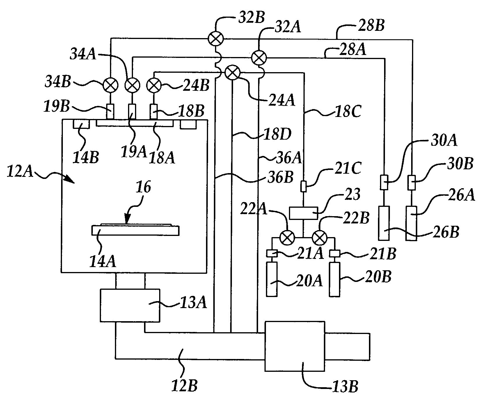
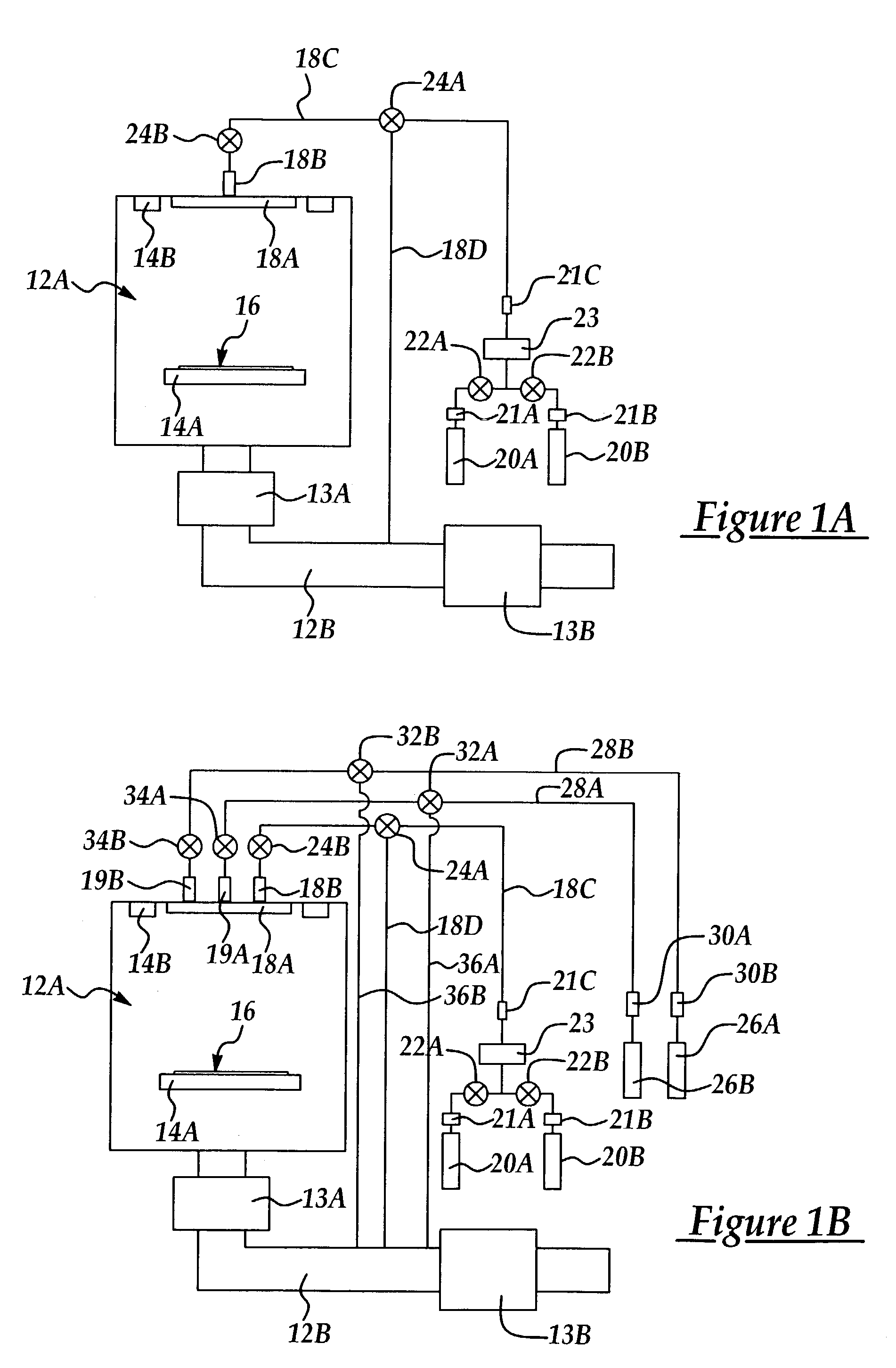
[0017]Although the apparatus and method of the present invention is explained with reference to a particular plasma reactor configuration, it will be appreciated that the reactant gas bypass system of the present invention may be used with any plasma reactor system for plasma enhanced chemical vapor deposition (PECVD). In addition, although the method of the present invention is explained with reference to an exemplary implementation of forming a silicon nitride layer over exposed copper containing semiconductor features it will be appreciated that the method of the present invention using the reactant gas bypass system of the present invention may be used in any PECVD process where a stable gas flow including a plasma may be advantageously maintained to prevent undesired reactant deposition and deposition film thickness non-uniformities during the deposition process.

[0018]Referring to FIG. 1A, a portion of a reactant gas bypass system is shown together with an exemplary plasma reac...


PUM

PropertyMeasurementUnit
Fractionaaaaaaaaaa
Thicknessaaaaaaaaaa
Flow rateaaaaaaaaaa

Abstract

A method and reactant gas bypass system for carrying out a plasma enhanced chemical vapor deposition (PECVD) process with improved gas flow stability to avoid unionized reactant precursors and thickness non-uniformities the method including providing a semiconductor process wafer having a process surface within a plasma reactor chamber for carrying out at least one plasma process; supplying at least one reactant gas flow at a selected flow rate to bypass the plasma reactor chamber for a period of time to achieve a pre-determined flow rate stability; and, redirecting the at least one reactant gas flow into the plasma reactor chamber to carry out the at least one plasma process.

Description

FIELD OF THE INVENTION[0001]This invention generally relates to a gas feed system and method for a plasma enhanced chemical vapor deposition (PECVD) apparatus and method and more particularly to a gas feed system to improve gas flow characteristics during PECVD deposition to improve film deposition by avoiding reactions of unionized reactants and thickness non-uniformities.BACKGROUND OF THE INVENTION[0002]While there are many methods for depositing material in VLSI and ULSI technology, these methods maybe broadly classified into chemical vapor deposition (CVD) and physical vapor deposition (PVD). CVD is defined as the formation of a nonvolatile solid film on a substrate by the reaction of vapor phase reactants that contain the required chemical constituents of the solid film. The most common CVD deposition methods are atmospheric pressure CVD (APCVD), low pressure CVD (LPCVD), and plasma enhanced CVD (PECVD). PECVD is a preferred method where lower temperatures are required.[0003]Th...

Claims


Application Information

Patent Timeline
IPC IPC(8): C23C16/00C23C16/44C23C16/455C23C16/509
CPCC23C16/4412C23C16/509C23C16/45561C23C16/455
Inventor CHENG, YI-LUNGLIAO, MO-CHENTSAI, ERICWU, SZE-AUWANG, YING-LUNG
Owner TAIWAN SEMICON MFG CO LTD
Why Eureka
Try Eureka