
Method of fabricating a rat's nest RFID antenna

a radio frequency identification and antenna technology, applied in the field of methods of fabricating rat's nest radio frequency identification (rfid) antennas, can solve the problems of large active rfid tags, more expensive than passive rfid tags, and the rfid chip b> will only offer a very limited range, and achieve the effect of low cost and little to the cos

Inactive Publication Date: 2007-12-04
ROUND ROCK RES LLC
View PDF12 Cites 64 Cited by
  • Summary
  • Abstract
  • Description
  • Claims
  • Application Information

AI Technical Summary

Benefits of technology

"The present invention solves the need for a more cost-effective and performance-oriented RFID tag design. The method involves connecting multiple antennas to previously fabricated RFID chips on a carrier substrate, resulting in a rat's nest of antennas. This design allows for the separation of each RFID chip, allowing for individual processing. The antennas can be connected in a predetermined order, and the resulting RFID tags can be easily attached to a host object. The use of low-cost wire bonding techniques and materials like aluminum or copper makes the antenna additionally cost-effective. Overall, this design offers a balance of cost and performance for RFID tags."

Problems solved by technology

Due to the requirement of a power source, active RFID tags are typically larger and more costly than passive RFID tags.
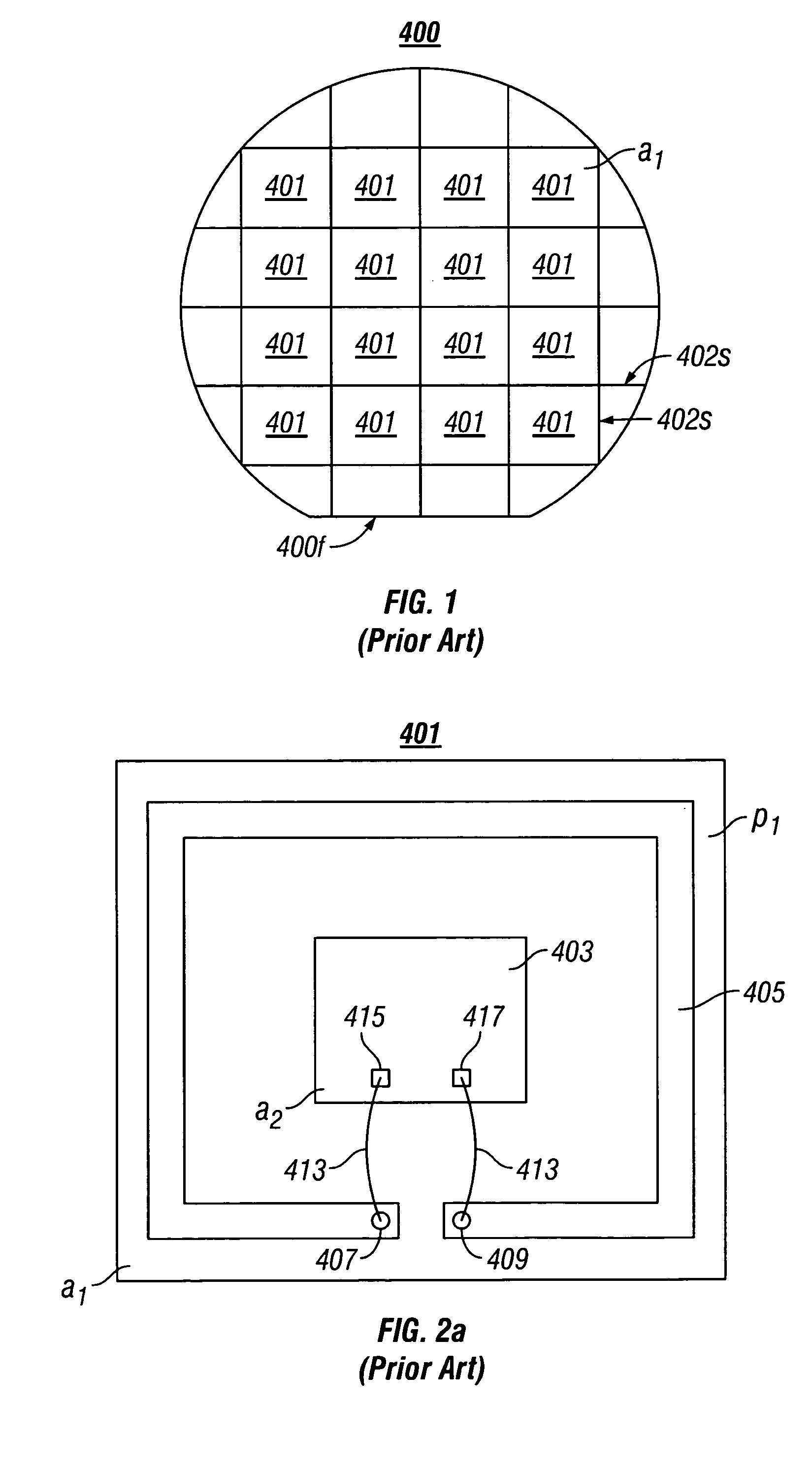
However, one disadvantage of the on-chip antenna 405 is that unless the chip 401 is large, the on-chip antenna 405 will offer only a very limited range.
Another disadvantage of on-chip antennas is that scaling of the RFID chip 401 to smaller chip sizes (i.e. reducing the area a1 thereby reducing tag cost) is largely precluded because shrinking the on-chip antenna 405 will seriously impact the range of the RFID chip 401 and / or reduce a data rate at which the information is transmitted from the RFID chip 401 to the RFID reader.
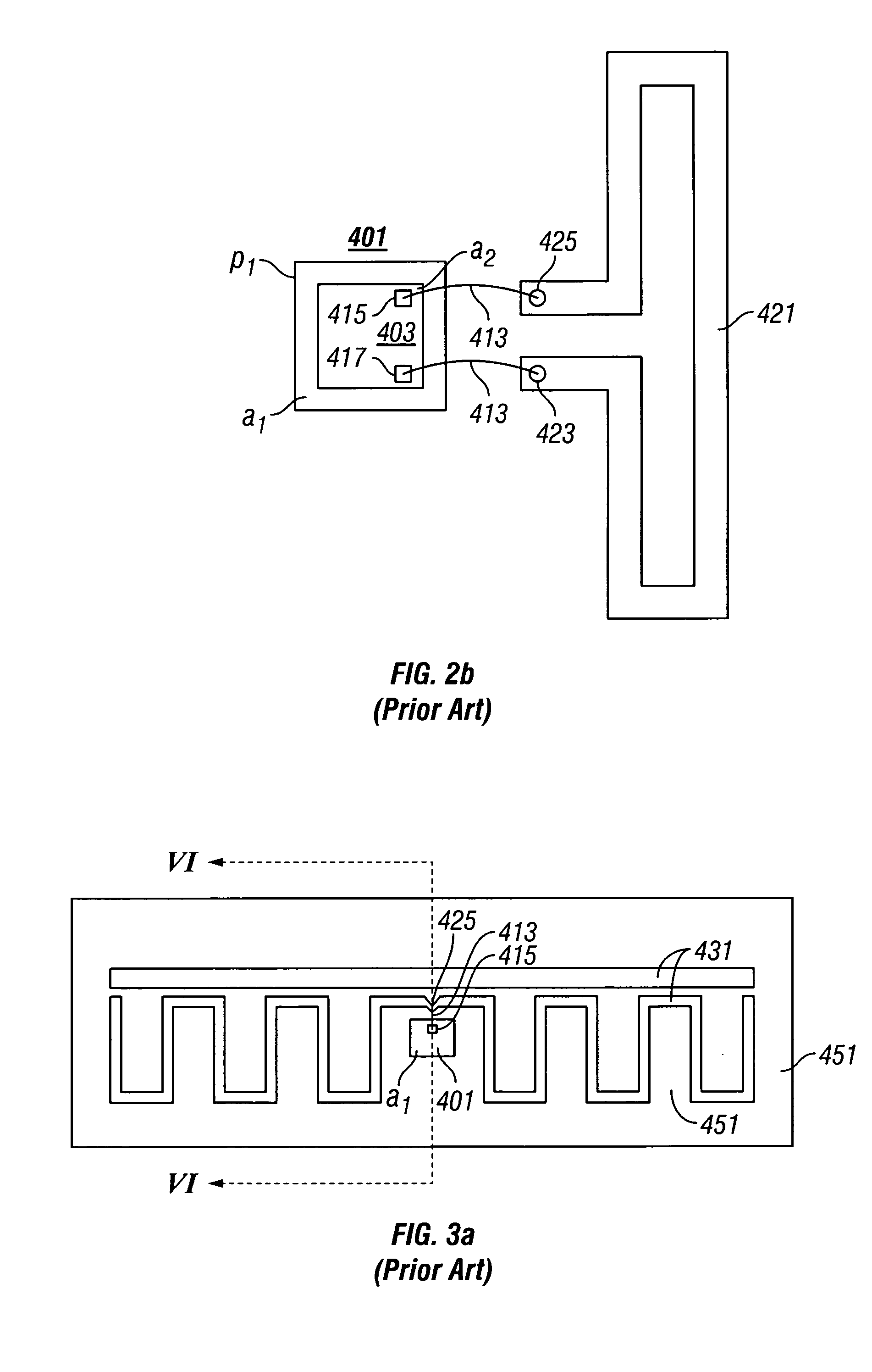
On the other hand, by using an external antenna as depicted in FIGS. 2b, 3a, and 3b, the range of the RFID chip 401 can be greatly increased, but at a substantial increase in tag cost.
Consequently, there exists a need for a RFID tag with a cost that approaches that of an on-chip antenna, but with a performance approaching that of a separately fabricated and much more expensive external antenna.

Method used


Image

  • Method of fabricating a rat's nest RFID antenna
  • Method of fabricating a rat's nest RFID antenna
  • Method of fabricating a rat's nest RFID antenna

Examples


Embodiment Construction

[0037]In the following detailed description and in the several figures of the drawings, like elements are identified with like reference numerals.

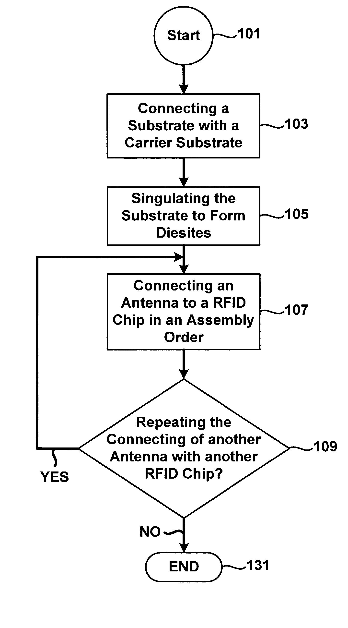
[0038]As shown in the drawings for purpose of illustration, the present invention is embodied in method of fabricating an antenna on a substrate including a plurality of previously fabricated RFID chips.

[0039]In FIGS. 5a and 5b, a substrate 11 includes a plurality of RFID chips 21 that have been previously fabricated on the substrate 11. Accordingly, one of ordinary skill in the art will appreciate that the RFID chips 21 can be fabricated using processes that are well understood in the microelectronics art and that the RFID chips 21 can include RF circuitry, analog circuitry, and digital circuitry. The substrate 11 can be made from a material including but not limited to a semiconductor material, silicon (Si), and a silicon wafer such as the type commonly used in the fabrication of microelectronic devices. The substrate 11 can have a shape...


PUM

PropertyMeasurementUnit
sizeaaaaaaaaaa
area A1aaaaaaaaaa
area A1aaaaaaaaaa

Abstract

A method of fabricating a radio frequency identification (RFID) antenna on a substrate is disclosed. The antenna is fabricated on a substrate that includes already fabricated RFID chips. The substrate is connected with a carrier substrate and singulated to separate the plurality of RFID chips into a plurality of diesites. The antenna is connected to a RFID chip in an assembly order to form an a RFID tag. The method is repeated such that each successively connected antenna overlaps a previously connected antenna.

Description

FIELD OF THE INVENTION[0001]The present invention relates generally to a method of fabricating a rat's nest radio frequency identification (RFID) antenna. More specifically, the present invention relates to a method of fabricating a RFID antenna on a RFID chip die while the die is still attached to a substrate.BACKGROUND OF THE ART[0002]Radio frequency identification (RFID) is a technology that has been in use since the 1940's where military aircraft carried large transponders as part of an IFF (Identify Friend-or-Foe) system. The transponder received electrical power from the aircraft and was thus an active RFID transponder. When a radar signal interrogated the transponder the transponder would generate a specific radio frequency signal that identified the aircraft as a “friendly” aircraft. This IFF system prevented otherwise friendly aircraft from being shot down by other friendly aircraft or friendly military forces.[0003]State of the art microelectronics technology now make it p...

Claims


Application Information

Patent Timeline
Patent Type & Authority Patents(United States)
IPC IPC(8): H01P11/00G06K19/077H01R43/00
CPCG06K19/07718G06K19/0775H01L24/48G06K19/07749Y10T29/4913H01L2223/6611H01L2223/6677H01L2224/05599H01L2224/45124H01L2224/45147H01L2224/48091H01L2224/4813H01L2224/48137H01L2224/48464H01L2224/48699H01L2924/01005H01L2924/01006H01L2924/01013H01L2924/01014H01L2924/01015H01L2924/01029H01L2924/01082H01L2924/014H01L2924/09701H01L2924/1433Y10T29/49016Y10T29/49018Y10T29/49117H01L2924/10253H01L2224/48799H01L2924/00014H01L2924/01033H01L2924/01019H01L2924/00H01L24/45H01L2224/05554
Inventor HAMBURGEN, WILLIAM
Owner ROUND ROCK RES LLC
Learn More