

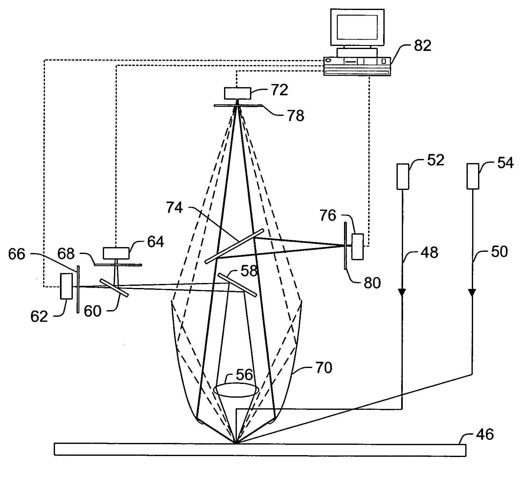
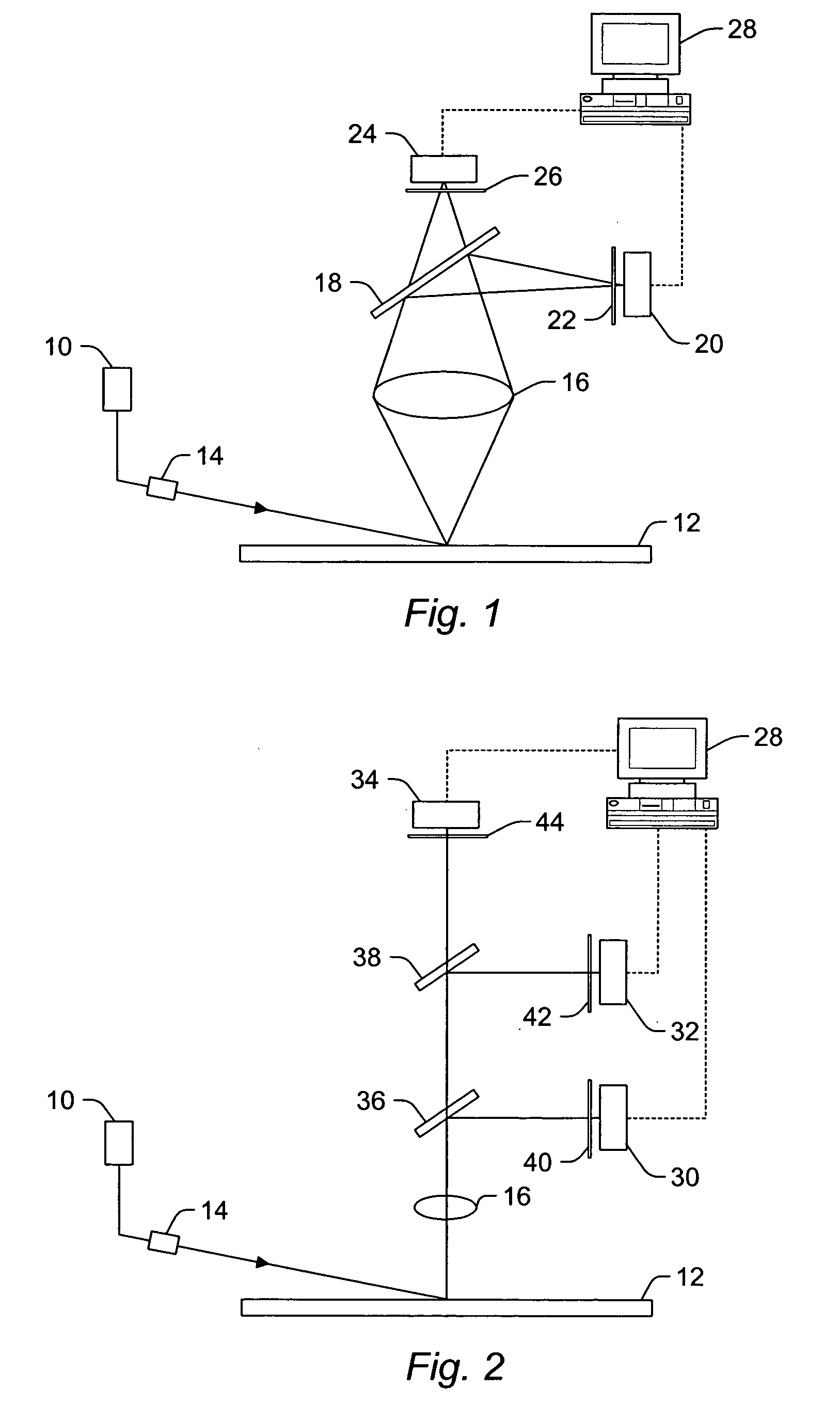
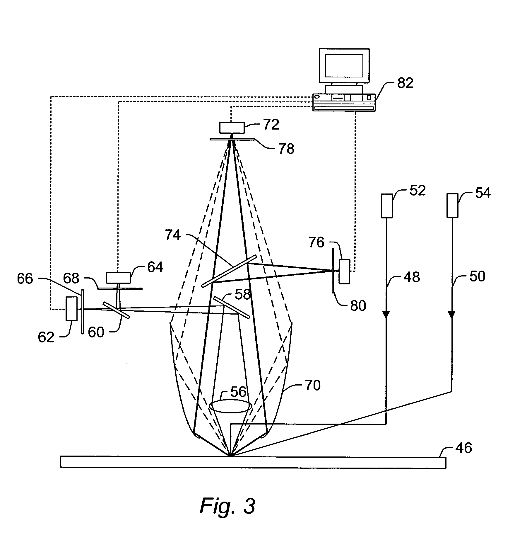
Methods and systems for inspecting a specimen using light scattered in different wavelength ranges
a technology of light scattering and specimens, applied in the direction of optical radiation measurement, instruments, spectrometry/spectrophotometry/monochromators, etc., can solve the problems of random defects, defects such as film thickness variation or lateral dimension variation, and particulate contamination and pattern defects being introduced into semiconductor devices
- Summary
- Abstract
- Description
- Claims
- Application Information
AI Technical Summary
Benefits of technology
Problems solved by technology
Method used
Image

Examples
example
Effect of Fluorescence Filter on Detection Sensitivity with Ultraviolet Illumination
[0100]Various wafers with different types of materials formed thereon as unpatterned films were inspected using ultraviolet illumination and visible illumination. The inspection systems used to perform the different inspections were similarly configured other than the illumination type. The ultraviolet illumination had a wavelength of 355 nm and a power of 350 mW. The visible illumination has a wavelength of 488 nm and a power of 75 mW. As can be seen from Table 1, the ultraviolet illumination provided increased sensitivity for some material types in comparison with visible illumination. The sensitivities are reported as nm latex sphere equivalent (LSE) thresholds using estimates from defect histograms and detectable PSL sizes. In addition, the different wafer types were also inspected using the ultraviolet illumination described above in addition to using a fluorescence filter to filter the detected...
PUM
 Abstract
Description
Claims
Application Information