Source follower and current feedback circuit thereof

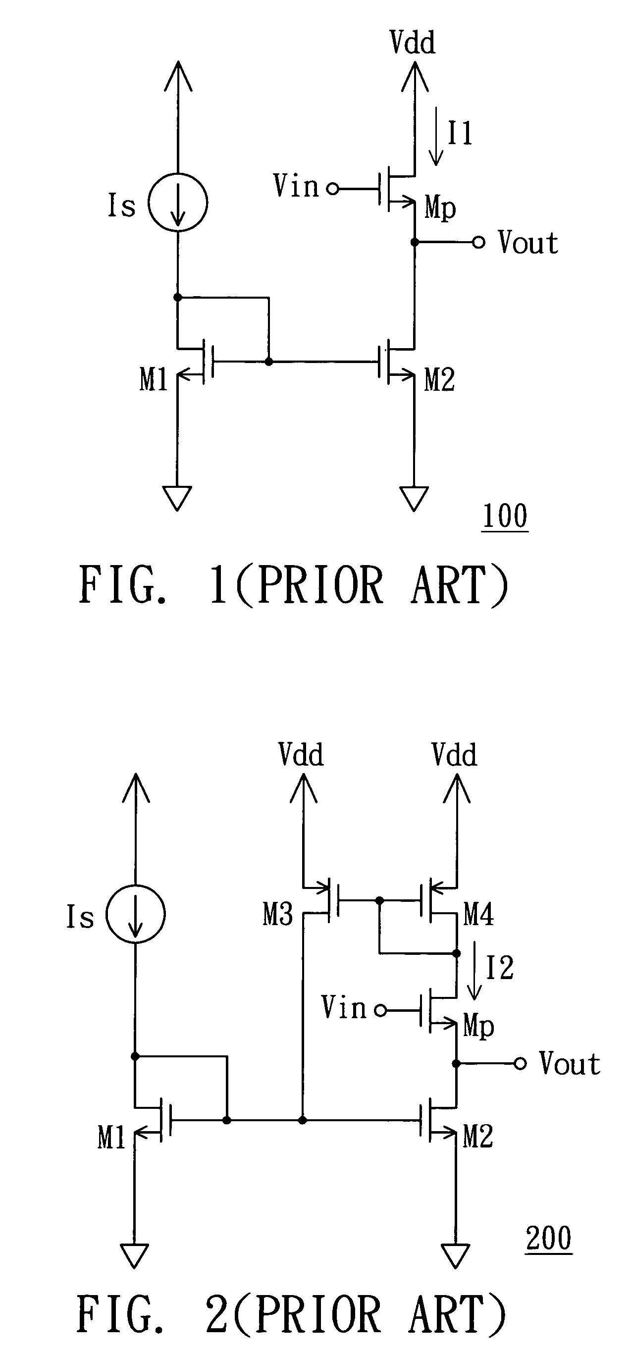
a current feedback circuit and source follower technology, applied in the field of source follower, can solve the problems of low operation voltage of the miniaturized integrated circuit, signal distortion of the output signal vout, and inability to stabilize the current flowing through the nmos transistor mb>2/b>, so as to prevent the distortion of the output signal

Active Publication Date: 2007-12-04
REALTEK SEMICON CORP
View PDF6 Cites 7 Cited by
  • Summary
  • Abstract
  • Description
  • Claims
  • Application Information

AI Technical Summary

Benefits of technology

[0007]It is therefore an object of the invention to provide a source follower using a current feedback circuit to prevent distortion of the output signal.

Problems solved by technology

Therefore, due to the channel length modulation effect, the current I1 flowing through the NMOS transistor M2 will not be stable.
Because the current I1 change causes variation of the voltage drop (Vgs) between the gate and the source of the NMOS transistor Mp, that is, the voltage difference between the input signal Vin and the output signal Vout, the input signal Vin cannot vary synchronously with the output signal Vout, thereby resulting in signal distortion of the output signal Vout.
However, this will lower down the operational voltage of the miniaturized integrated circuit.

Method used


Image

  • Source follower and current feedback circuit thereof
  • Source follower and current feedback circuit thereof
  • Source follower and current feedback circuit thereof

Examples


Embodiment Construction

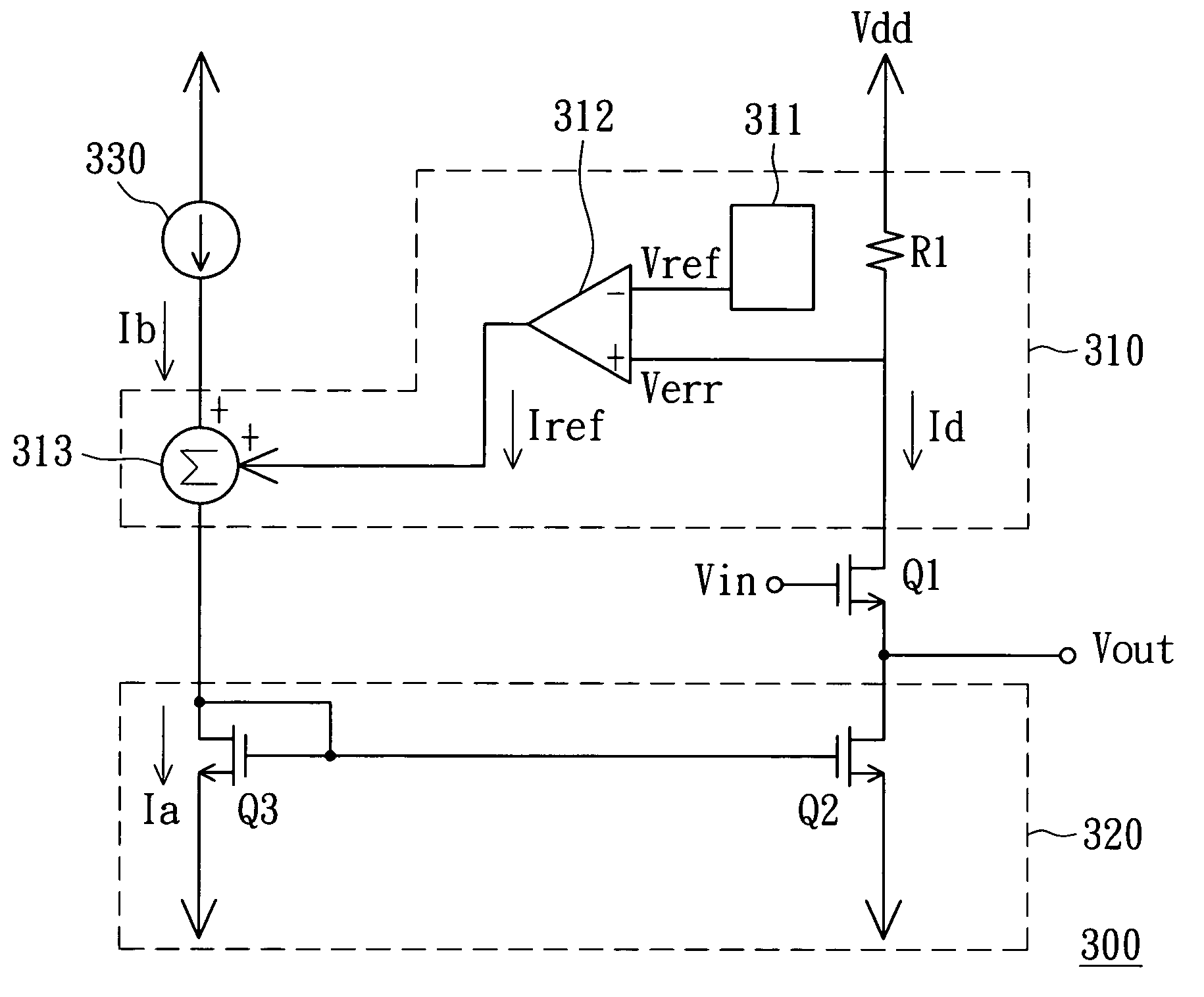
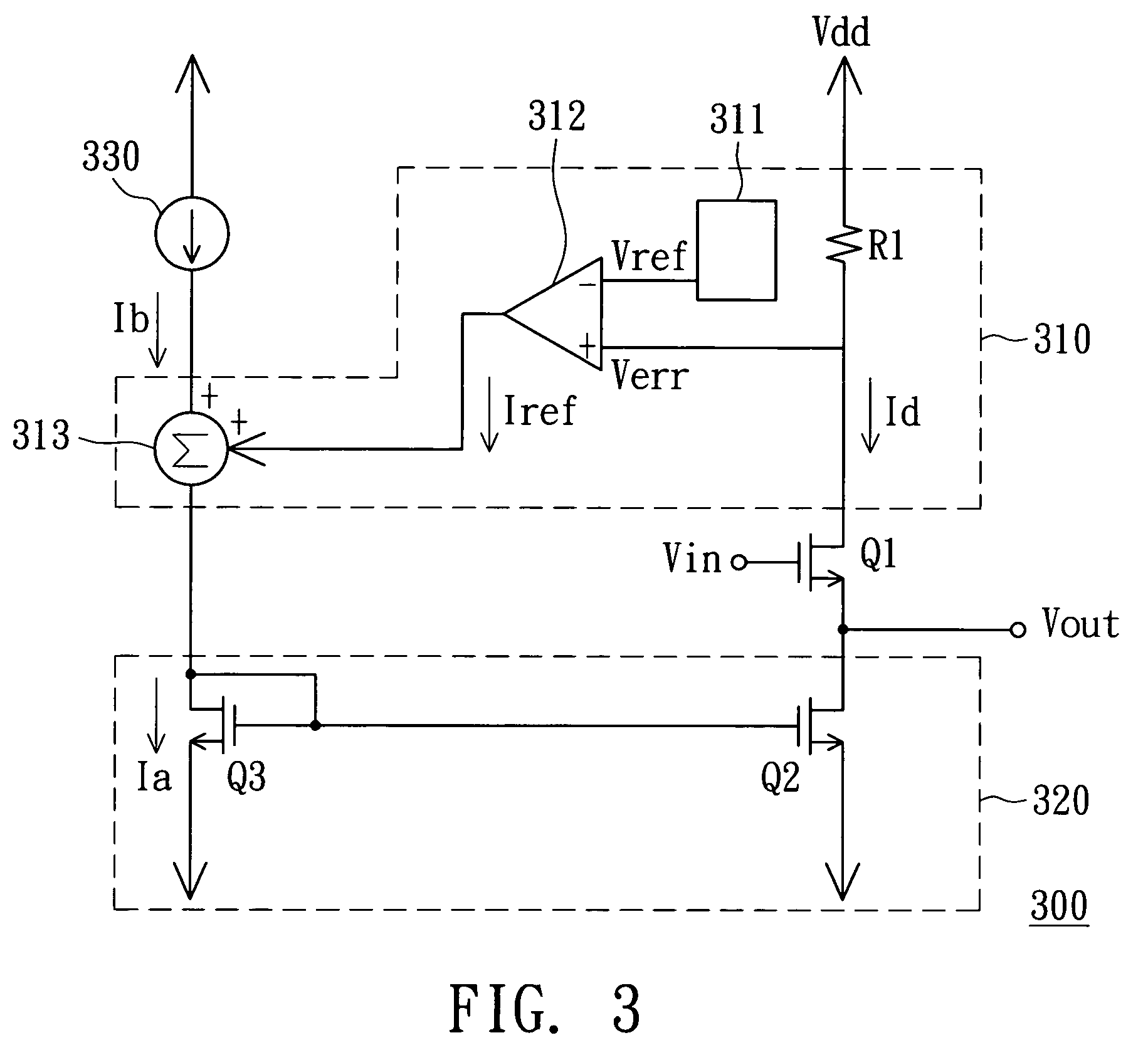
[0016]Referring to FIG. 3, a circuit diagram of a source follower according to a preferred embodiment of the invention is shown. The source follower 300 includes a NMOS transistor, a current feedback circuit 310, and a current mirror 320. The NMOS transistor has a gate for receiving an input signal Vin, and a source for outputting an output signal Vout. The current mirror substantially stabilizes the drain current Id of the NMOS transistor Q1 to prevent distortion of the output signal Vout according to a signal outputted by the current feedback circuit 310.

[0017]The current feedback circuit 310 includes a resistor R1, an operational amplifier 312, a reference voltage generator 311, and an adder 313. The resistor R1 has a first terminal coupled to a high-level voltage Vdd and a second terminal coupled to the drain of the NMOS transistor Q1 and the operational amplifier 312. The second terminal has an error voltage Verr equal to the difference of the voltage Vdd and the voltage drop a...


PUM


Abstract

A current feedback circuit is used in the source follower. The source follower includes a first MOS transistor and a current mirror. The first MOS transistor has a gate receiving an inputting signal and a source outputting an output signal. A drain current flows through the first MOS transistor. The current mirror generates the drain current according to an adding current. The current feedback circuit is used for stabilizing the drain current to a constant value substantially. The current feedback circuit includes a passive component and an operational amplifier. The passive component has a first end and a second end, which has an error voltage when a corresponding current flows through the passive component. The magnitude of the corresponding current changes with the magnitude of the drain current. The operational amplifier outputs a reference signal to adjust the adding current according to the error voltage and a reference voltage.

Description

[0001]This application claims the benefit of Taiwan application Serial No. 93139232, filed Dec. 16, 2004, the subject matter of which is incorporated herein by reference.BACKGROUND OF THE INVENTION[0002]1. Field of the Invention[0003]The invention relates in general to a source follower, and more particularly to a source follower and current feedback circuit thereof.[0004]2. Description of the Related Art[0005]Source follower is a widely applied circuit nowadays. As shown in FIG. 1, the source follower 100 includes a current source Is, an N-type metal oxide semiconductor (NMOS) transistor M1, a NMOS transistor M2, and a NMOS transistor Mp. A current I1 flows through the NMOS transistors M2 and Mp. Owing that NMOS transistors are influenced by channel length modulation effect, the current I1 is not stable as ideal, thereby influencing the output signal Vout. For example, when the input signal Vin varies, the output signal Vout will have the same phase change with the input signal Vin...

Claims


Application Information

Patent Timeline
Patent Type & Authority Patents(United States)
IPC IPC(8): H03F1/30
CPCH03F1/3205H03F1/34H03F3/347H03F3/505H03F3/345H03F2200/135
Inventor TU, CHUAN-PING
Owner REALTEK SEMICON CORP
Why Eureka
Try Eureka