Liquid crystal display panel

a liquid crystal display panel and display panel technology, applied in static indicating devices, instruments, non-linear optics, etc., can solve the problems of high power consumption, deterioration of display quality of liquid crystal display panels, and more deterioration of display quality, so as to reduce parasitic capacitor capacitance deviation, and minimize asymmetric light leakage

Active Publication Date: 2007-12-04
LG DISPLAY CO LTD
View PDF4 Cites 20 Cited by
  • Summary
  • Abstract
  • Description
  • Claims
  • Application Information

AI Technical Summary

Benefits of technology

[0026]An advantage of the present invention is to provide a liquid crystal display panel capable of reducing a capacitance of a parasitic capacitor between a pixel electrode and a data line.
[0027]Another advantage of the present invention is to provide a liquid crystal display panel capable of reducing a capacitance deviation of a parasitic capacitor between a left and right pixel electrode and a data line.
[0028]Another advantage of the present invention is to provide a liquid crystal display panel capable of minimizing an asymmetric light leakage between a left and right pixel electrode and a data line.
[0029]Another advantage of the present invention is to provide a liquid crystal display panel capable of minimizing a crosstalk caused by a parasitic capacitor between a pixel electrode and a data line.

Problems solved by technology

However, the dot inversion driving method has a disadvantage because the polarity of the pixel voltage signal applied from the data driver to the data line is inverted in the horizontal and vertical direction, an amount of the fluctuation of a pixel signal, i.e., the frequency of a pixel signal, is higher than that of the other inversion methods, thus power consumption is high.
Due to a coupling effect caused by the first and the second parasitic capacitors Cdp1 and Cdp2, a pixel signal supplied to the data line DLk and the pixel electrode P1 and P2 is distorted, which results in the display quality of the liquid crystal display panel being deteriorated.
An asymmetric light leakage caused by the first and second parasitic capacitors induces a display quality that is more deteriorated.

Method used


Image

  • Liquid crystal display panel
  • Liquid crystal display panel
  • Liquid crystal display panel

Examples


first embodiment

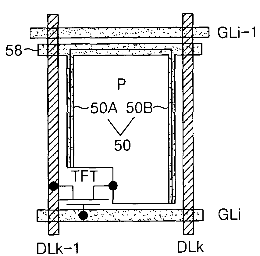
[0064]FIG. 7 is a plan view illustrating a structure of the liquid crystal display panel according to the present invention. The liquid crystal display panel shown in FIG. 7 is identical to the liquid crystal display panel shown in FIG. 4 except that it further includes a common line connected to a shield pattern 50. Therefore, a detailed explanation as to the elements identical to those in FIG. 4 will be omitted.

[0065]The shield pattern 50 overlapping both side portions of pixel electrodes P1 to P4 is electrically connected to the common line 54 crossing the pixel electrodes P1 to P4. The common line 54 supplies a bias voltage, for example, a common voltage Vcom referenced to drive a liquid crystal or a ground voltage GND, to the shield pattern 50. In the event that the shield pattern 50 is biased, as shown in FIG. 7, any effect caused by the pixel signal of the data line DL on each of the liquid crystal cells 32 is reduced in contrast with the shield pattern 30, of FIG. 4, having ...

second embodiment

[0079]FIG. 11 illustrates a part of the liquid crystal display panel according to the present invention. The liquid crystal display panel shown in FIG. 11 is identical, except that it further has an expanded part 74A having an enlarged line width for enlarging the area overlapped between a common line 74 and pixel electrodes P1 to P4, when compared to the liquid crystal display panel shown in FIG. 7. Therefore, explanation of elements identical to those of FIG. 7 will be omitted.

[0080]A shield pattern 70 shown in FIG. 11 is connected to the common line 74 crossing the pixel electrodes P1 to P4. A bias voltage, for example, a common voltage Vcom referenced to drive a liquid crystal or a ground voltage GND is provided to the shield pattern 70. Although the base voltage is not applied to the shield pattern 70, all of the shield patterns 70 independently formed for each liquid crystal cell 72 are connected by the common line 74. Accordingly, an effect on the shield pattern 70 by the dat...

third embodiment

[0090]FIG. 13 illustrates the present invention. The liquid crystal display panel shown in FIG. 13 is identical, except that a shield pattern 100, which is connected to a common line 104, is electrically connected to the gate line GLi−1 of a previous stage, to the liquid crystal display panel shown in FIG. 7. Therefore, an explanation on elements identical to those of FIG. 7 will be omitted to avoid duplication.

[0091]The shield pattern 100 shown in FIG. 13 is connected to the common line 104 that crosses the pixel electrodes P1 to P4 and is electrically connected to the gate line GLi−1 of a previous stage. Accordingly, gate signals to be supplied to the gate line GL, that is, a high gate voltage for turning-on the thin film transistor TFT and a low gate voltage for turning-off the TFT are supplied to the shield pattern 100 and the common line 104 as a bias signal. In general, the high gate voltage is supplied only for a driving period of one horizontal line within one frame, and the...


PUM

PropertyMeasurementUnit
widthaaaaaaaaaa
widthaaaaaaaaaa
widthaaaaaaaaaa

Abstract

A liquid crystal display panel capable of reducing a capacitance of a parasitic capacitor between a data line and a pixel electrode. The liquid crystal display panel comprises: a thin film transistor at a crossing of a gate line and a data line, liquid crystal cells including a pixel electrode connected to the thin film transistor; first shield patterns in the liquid crystal cells, each shield pattern being parallel to the data line without overlapping the data line, wherein the shield patterns are insulated from and overlap with an outer portion of the pixel electrode; and a common line arrayed to connect the shield patterns for each the liquid crystal cell.

Description

[0001]This application claims the benefit of Korean Patent Application No. P2003-41122 filed on Jun. 24, 2003,which is hereby incorporated by reference for all purposes as if fully set forth herein.BACKGROUND OF THE INVENTION[0002]1. Field of the Invention[0003]The present invention relates to a liquid crystal display device. More particularly, the present invention relates to a liquid crystal display panel capable of minimizing crosstalk by using a parasitic capacitor between a pixel electrode and a data line.[0004]2. Discussion of the Related Art[0005]Generally, a liquid crystal display (LCD) controls the light transmittance of liquid crystal with dielectric anisotropy by using an electric field to display a picture. To this end, the LCD includes a liquid crystal display panel having liquid crystal cells arranged in a matrix, and a drive circuit for driving the liquid crystal display panel.[0006]The drive circuit for the liquid crystal display drives the liquid crystal display pan...

Claims


Application Information

Patent Timeline
Patent Type & Authority Patents(United States)
IPC IPC(8): G02F1/1343G02F1/1333G02F1/1362
CPCG02F1/1362G09G2320/0209G02F2001/136218G02F1/136218G02F1/1343
Inventor SONG, HONG SUNGYUN, SAI CHANGYUN, SANG CHANGLEE, JAE WOO
Owner LG DISPLAY CO LTD
Why Eureka
Try Eureka