Mounting structure of high-frequency semiconductor apparatus and its production method

a high-frequency semiconductor and mounting structure technology, applied in the field of high-frequency circuits, can solve the problems of difficult mass production and production cost reduction, difficult to produce low-cost mmic, and difficult to determine the shape of the resonator and its relative position, etc., to achieve stable frequency characteristics, low price, and easy positioning of the dielectric resonator and the high-frequency transmission lin

Inactive Publication Date: 2007-12-11
HITACHI LTD
View PDF14 Cites 7 Cited by
  • Summary
  • Abstract
  • Description
  • Claims
  • Application Information

AI Technical Summary

Benefits of technology

[0022]According to the present invention, it will be appreciated that a high-precision positioning between the dielectric resonator and the high-frequency transmission line can be made easier, and that high-performance oscillators having a stable frequency characteristic can be produced at a low price.

Problems solved by technology

In the prior art of the adhesive bonding method in which the resonator is bonded to the micro-strip transmission line connected to the oscillation part so as to establish the electro-magnetic coupling, there is such a problem that it is difficult to determine the shape of the resonator and its relative position to the micro-strip transmission line in order to satisfy the desired frequency and power as well as the designated phase noise.
As it is required that the precision for the geometrical dimension of the resonator to its designed target value is ±0.1% and that the precision for fixing the resonator to its designed position is ±5% of its geometrical dimension, as for the shape, it is necessary to trim the shape of the resonator by grinding the dielectric material, and as for the positioning, it is necessary to mount the resonator by the high-precision mounter, and thus, it has been difficult to operate the mass production and downsize the cost in production.
However, as the price per unit area of the materials such as GaAs used conventionally as the integrated circuit substrate in the high-frequency region is extremely high, it is difficult to produce the low-cost MMIC.
In this case, as the Q factor as the oscillator is reduced due to the dielectric loss even in the fact of using the dielectric material with high Q factor for the resonator, there is such a problem that the expected effect of high Q factor is not attained.

Method used


Image

  • Mounting structure of high-frequency semiconductor apparatus and its production method
  • Mounting structure of high-frequency semiconductor apparatus and its production method
  • Mounting structure of high-frequency semiconductor apparatus and its production method

Examples


Embodiment Construction

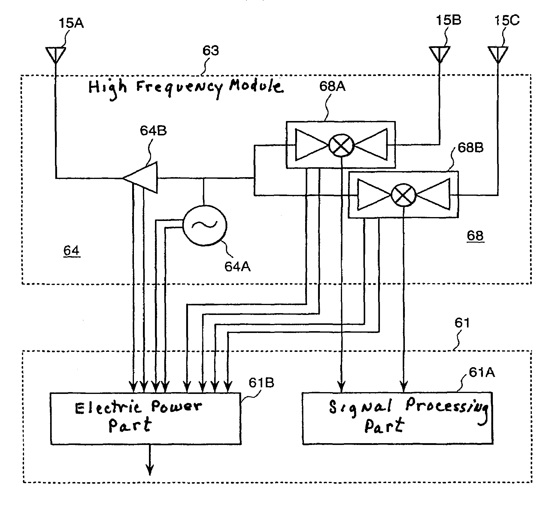
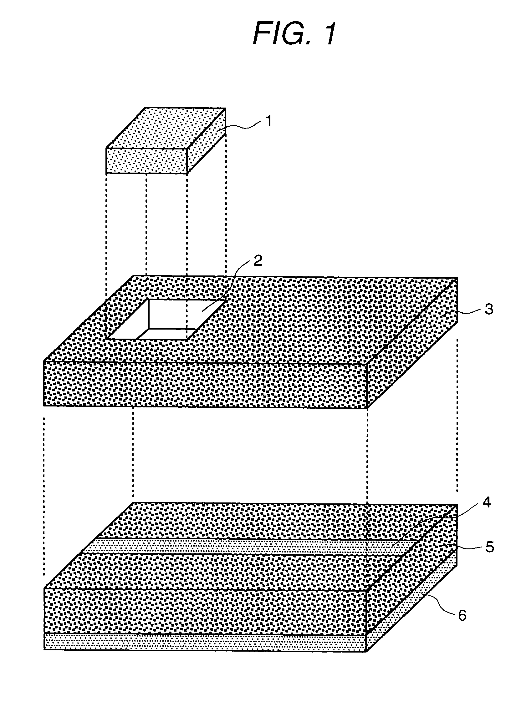
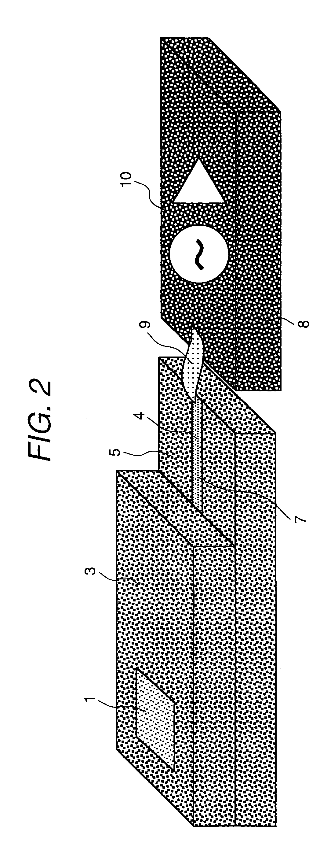
[0032]At first, for the first embodiment of the present invention, an external resonator, the structure of the oscillator using this resonator and its mounting method will be described below.

[0033]FIG. 1 is a perspective view illustrating the external appearance of the external resonator in the first embodiment of the present invention. The external resonator is composed of a couple of substrates comprising the first dielectric layer 5 and the second dielectric layer 3 laminated on the first layer, and the dielectric resonator 1. Both of the first dielectric layer 5 and the second dielectric layer 3 are composed of low dielectric constant material having a relative dielectric constant 10 or smaller. GND layer 6 composed of Ag / Pd, Ag, Au, Ag / Pt and the like is formed on one side of the first dielectric layer 5, and the transmission line 4 similarly composed of Ag / Pd, Ag, Au, Ag / Pt and the like is formed on the other side of the first dielectric layer. The hole part 2 is formed in the...


PUM

PropertyMeasurementUnit
dielectric constantaaaaaaaaaa
relative dielectric constantaaaaaaaaaa

Abstract

In a high-frequency circuit having a substrate having a high-frequency transmission line and an dielectric resonator formed on said substrate so that said dielectric resonator and said high-frequency transmission line may be coupled electro-magnetically to each other, a hole part or a cavity part is formed at a part of said substrate and a dielectric resonator is embedded in said hole part or said cavity part. In the same object, a high-frequency circuit having a dielectric resonator is produced by the step for forming a high-frequency transmission line on a substrate, the step for forming a hole part or a cavity part on a part of the substrate, and the step for mounting a dielectric resonator in the hole par formed on the surface of the substrate.

Description

[0001]This application is a divisional application of U.S. patent application Ser. No. 10 / 245,724, filed Sep. 18, 2002, now U.S. Pat. No. 6,771,150.BACKGROUND OF THE INVENTION[0002]The present invention relates to a high-frequency circuit having a built-in dielectric resonator and a oscillator using this high-frequency circuit, and their production method.[0003]In a frequency processing circuit for the high-frequency region such as microwave and extremely high frequency wave, it is required to reduce the phase noise in order to stabilize the frequency characteristic of the oscillator. In addition, it is effective to increase the load Q factor of the oscillator in order to reduce the phase noise. For example, increasing the Q factor ten times can reduce the phase noise by 1 / 100.[0004]Thus, using an dielectric material having a high Q factor for the material of the oscillator and shaping precisely the oscillator so as to have a desired resonant frequency, the adhesive agent with a low...

Claims


Application Information

Patent Timeline
Patent Type & Authority Patents(United States)
IPC IPC(8): G01S13/00H03B1/00G01S13/93C04B35/00H01P1/20H01P7/10H01P11/00H03B5/18H04B1/3822H04B1/40
CPCH01P11/008H01P7/10
Inventor SASADA, YOSHIYUKI
Owner HITACHI LTD
Why Eureka
Try Eureka