

Cleaning composition and method of cleaning a semiconductor device using the same
a technology of cleaning composition and semiconductor device, which is applied in the direction of chairs, instruments, applications, etc., can solve the problems of metal corrosion in the front end of line (feol), deterioration of the tungsten structure, and decrease of the efficiency and reliability of the semiconductor device,
Active Publication Date: 2007-12-18
SAMSUNG ELECTRONICS CO LTD
View PDF14 Cites 4 Cited by
- Summary
- Abstract
- Description
- Claims
- Application Information
AI Technical Summary
Benefits of technology
The present invention relates to a cleaning composition for semiconductor devices that includes an alkali solution, pure water, and a surfactant. The surfactant can be selected from a group of chemicals, such as butyl, isobutyl, isooctyl, nonyl phenyl, octyl phenyl, decyl, tridecyl, lauryl, myristyl, cetyl, stearyl, oleyl, licenoleyl, and behnyl groups. The composition can also include a metal corrosion inhibitor. The cleaning method involves cleaning the semiconductor device using this cleaning composition. The technical effect of this invention is to provide a more effective and efficient cleaning process for semiconductor devices.
Problems solved by technology
As patterns of the semiconductor device become small, the resistance thereof increases, and efficiency and reliability of the semiconductor device decrease.
The strong alkaline cleaning solution or the strong acid cleaning solution may cause metal corrosion in the front end of line (FEOL).
For examples, when the tungsten structure is cleaned using the SC1 cleaning solution or the SPM cleaning solution, hydrogen peroxide in the cleaning solutions corrodes tungsten in the tungsten structure.
Thus, when the tungsten structure of the semiconductor device is exposed, the above-mentioned cleaning solution may not be used for the semiconductor device.
When a semiconductor device is cleaned using above-mentioned cleaning solutions, reducing corrosion of tungsten as well as decreasing etched amount of polysilicon may be limited.
Method used
View moreImage
Smart ImageViewing Examples

Examples
example 1
[0046]Ammonia solution (manufactured by Aldrich Chemical Co. in USA) and about 0.1 weight percent of ammonium lauryl sulfate referred to as ALS (manufactured by Wako Pure Chemical Co. in Japan) as an anionic surfactant were mixed at room temperature to prepare a cleaning composition. The ammonia solution included about 0.27 weight percent of ammonia.
example 2
[0047]A cleaning composition was prepared in accordance with Example 1 as described above except the cleaning composition included about 0.2 weight percent of ALS.
Login to View More PUM
| Property | Measurement | Unit |
|---|---|---|
| weight percent | aaaaa | aaaaa |
| weight percent | aaaaa | aaaaa |
| weight percent | aaaaa | aaaaa |
Abstract
A cleaning composition comprises an alkali solution, pure water, and a surfactant represented by the following chemical formula: R1-OSO3—HA+ wherein R1 is one selected from a group consisting of a butyl group, an isobutyl group, an isooctyl group, a nonyl phenyl group, an octyl phenyl group, a decyl group, a tridecyl group, a lauryl group, a myristyl group, a cetyl group, a stearyl group, an oleyl group, a licenoleyl group and a behnyl group, and A is one selected from a group consisting of ammonia, ethanol amine, diethanol amine and triethanol amine.
Description
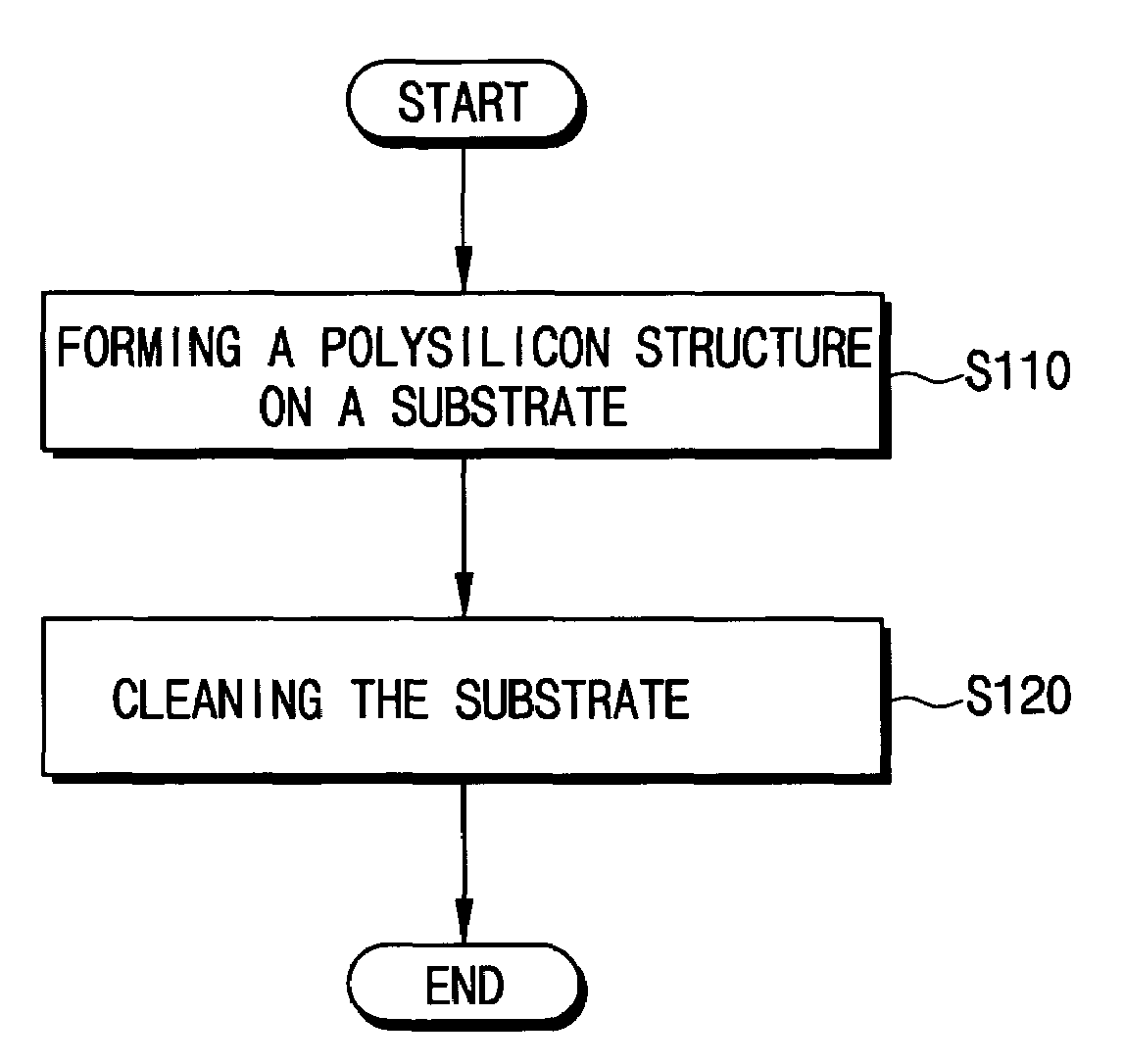
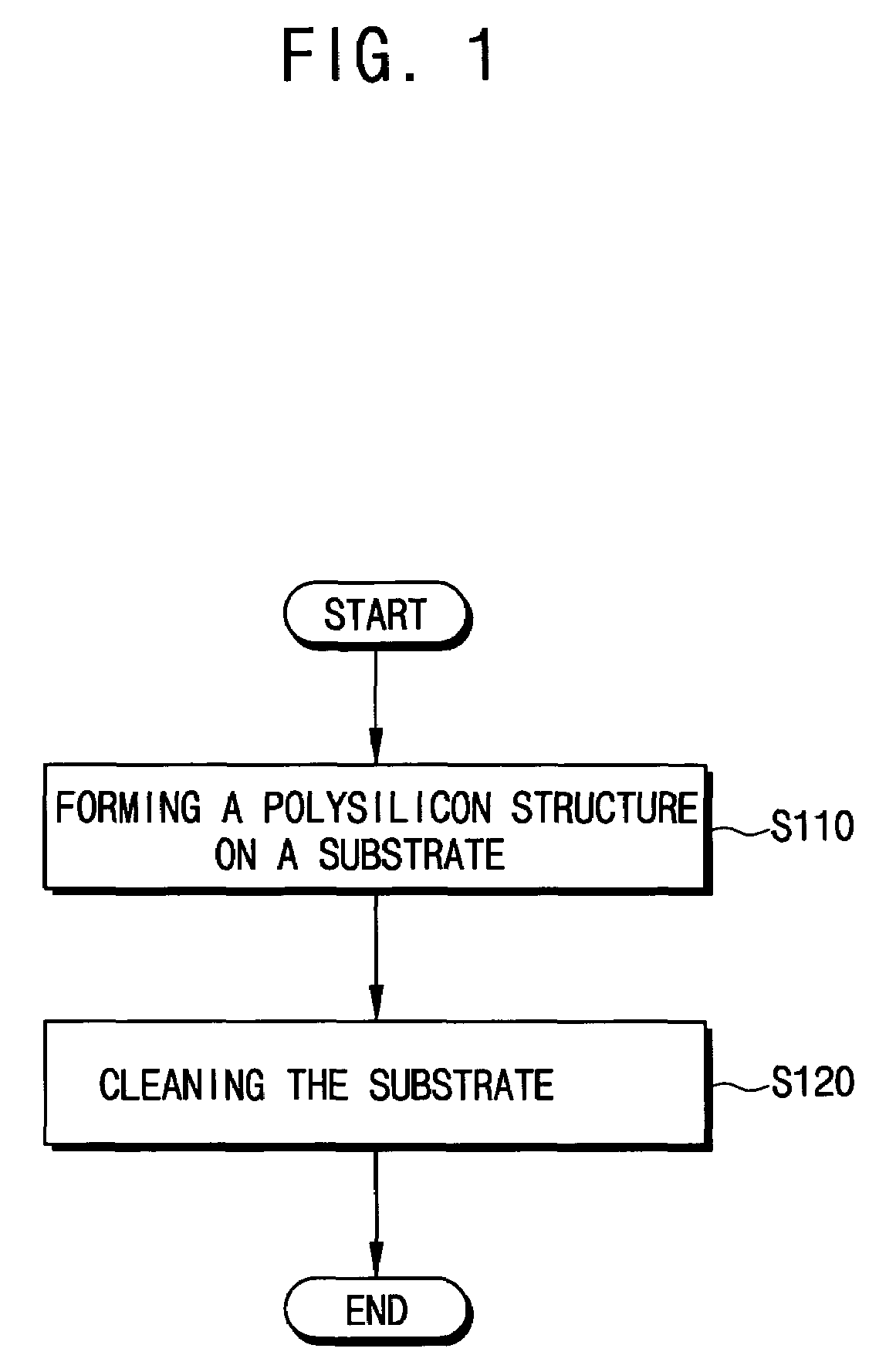
CROSS REFERENCE TO RELATED APPLICATION[0001]This application claims priority to Korean Patent Application No. 2004-4319 filed on Jan. 20, 2004, which is incorporated herein by reference in its entirety.BACKGROUND[0002]1. Technical Field[0003]The present disclosure relates to a cleaning composition and a method of cleaning a semiconductor device comprising the cleaning composition, and more particularly, to a cleaning composition that reduces damage to a structure of polysilicon and metal corrosion of a semiconductor device, and a method of cleaning the semiconductor device comprising the cleaning composition.[0004]2. Discussion of Related Art[0005]Highly integrated semiconductor devices having rapid response speed are generally used in information processing apparatuses. Technology of manufacturing the highly integrated semiconductor devices has been developed to improve such as an integration degree, reliability, and a response speed of the semiconductor device.[0006]As patterns of...
Claims
Login to View More Application Information
Patent Timeline
 Patent Type & AuthorityPatents(United States)
IPC IPC(8): C11D1/12C11D1/14C11D3/00C11D3/20C11D3/34C11D11/00
CPCC11D1/146C11D3/0073C11D3/2031H01L21/02071C11D3/3409C11D3/3427C11D11/0047C11D3/2055C11D2111/22A47G27/00A47C7/02
InventorMUN, CHANG-SUPHONG, CHANG-KICHOI, SANG-JUNHAN, WOO-SUNG
OwnerSAMSUNG ELECTRONICS CO LTD