Data communication method and data communication device and semiconductor device

a data communication and data communication technology, applied in the field of data communication methods and data communication devices and semiconductor devices, can solve the problems of deteriorating the performance of the whole system, ic and outside data transmission speeds becoming an issue, and the scaling of the mos is not easily applied, so as to reduce the delay of output buffers, reduce current change amounts, and increase the number of transmission lines

Inactive Publication Date: 2008-01-15
RENESAS ELECTRONICS CORP
View PDF15 Cites 4 Cited by
  • Summary
  • Abstract
  • Description
  • Claims
  • Application Information

AI Technical Summary

Benefits of technology

[0008]When transition takes place only in an output signal of one of the plurality of output buffers, a current does not flow so much between the power supply line for applying the operation voltage to the output buffer and the ground line, and a current change amount is small. Consequently, a potential difference appearing between both ends of the inductance depends on the change amount of the flowing current and decreases. In the case where the current change amount is small as described above, the potential difference between the power supply line for applying the operation voltage to the output buffer and the ground line does not decrease so much. Therefore, the current driving force of the output buffer does not decrease so much, and a delay of the output buffer is reduced.
[0009]As described above, a difference in delay time of the output buffer occurs between the case where the number of output signals in which transition occurs is large and the case where the number is small. The jitter causes decrease in the timing window, and it disturbs increase in the transmission speed. Although it is easily inferred from analogy, the larger the number of transmission lines is, the larger the jitter in the transmission lines due to the simultaneous switching noise is, and increase in the number of transmission lines can be also prevented.

Problems solved by technology

However, the scaling of the MOS is not easily applied to an interface between an IC and the outside and, accordingly, the data transmission speeds of the IC and the outside is becoming an issue.
Particularly, in communication between ICs (integrated circuits) on the same printed circuit board (PC board), the communication speed is insufficient and it is causing deterioration of the performance of the whole system.
The problem of separately transmitting the clock signal and data is constraint of timings.
It disturbs increase in the data transfer speed per transmission line in the parallel link.
Fluctuations between the power supply line and the ground line are called simultaneous switching noise.
When the power supply voltage decreases, the current driving force of the output buffer decreases, and a delay of the output buffer increases.

Method used


Image

  • Data communication method and data communication device and semiconductor device
  • Data communication method and data communication device and semiconductor device
  • Data communication method and data communication device and semiconductor device

Examples


Embodiment Construction

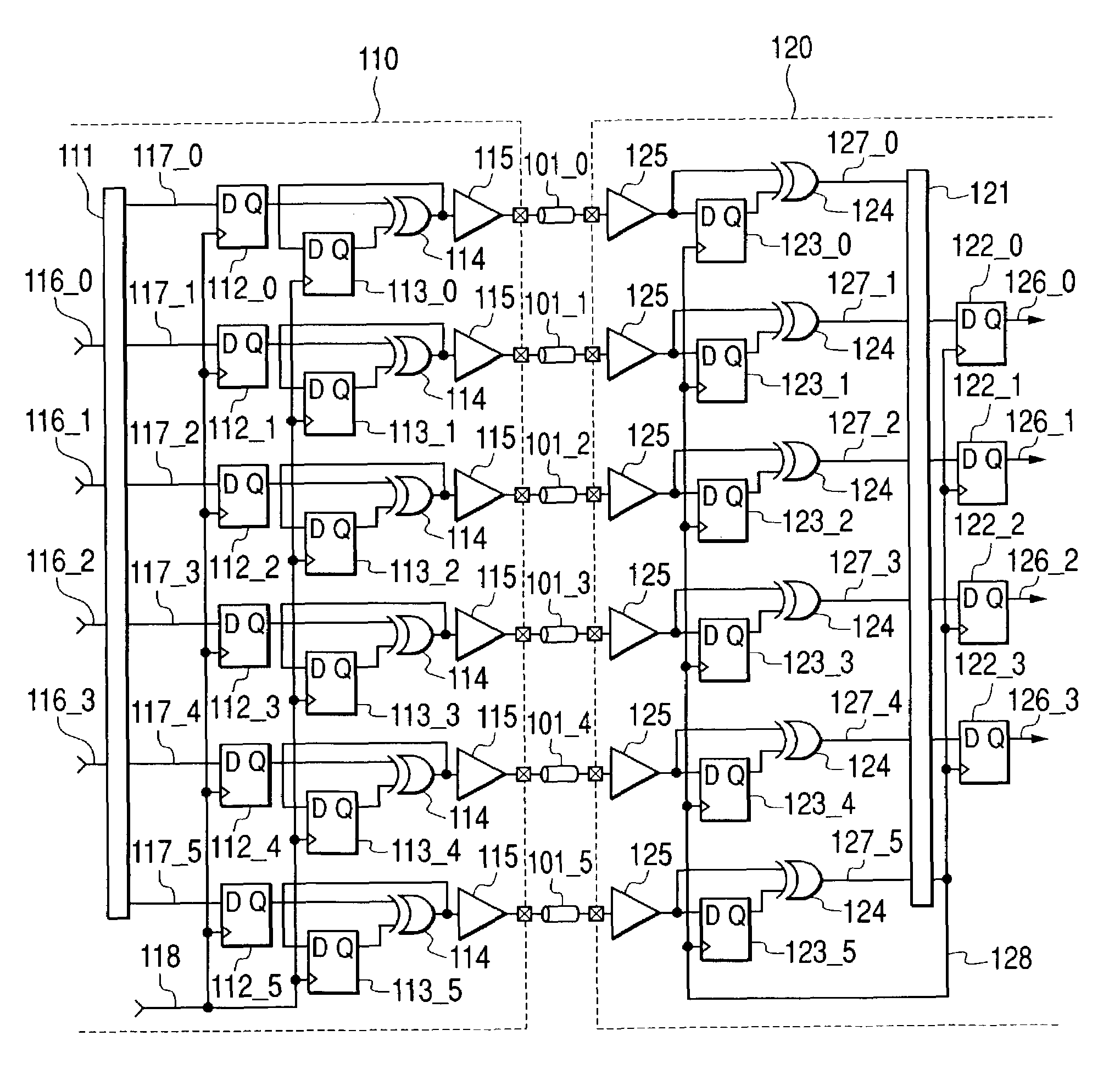
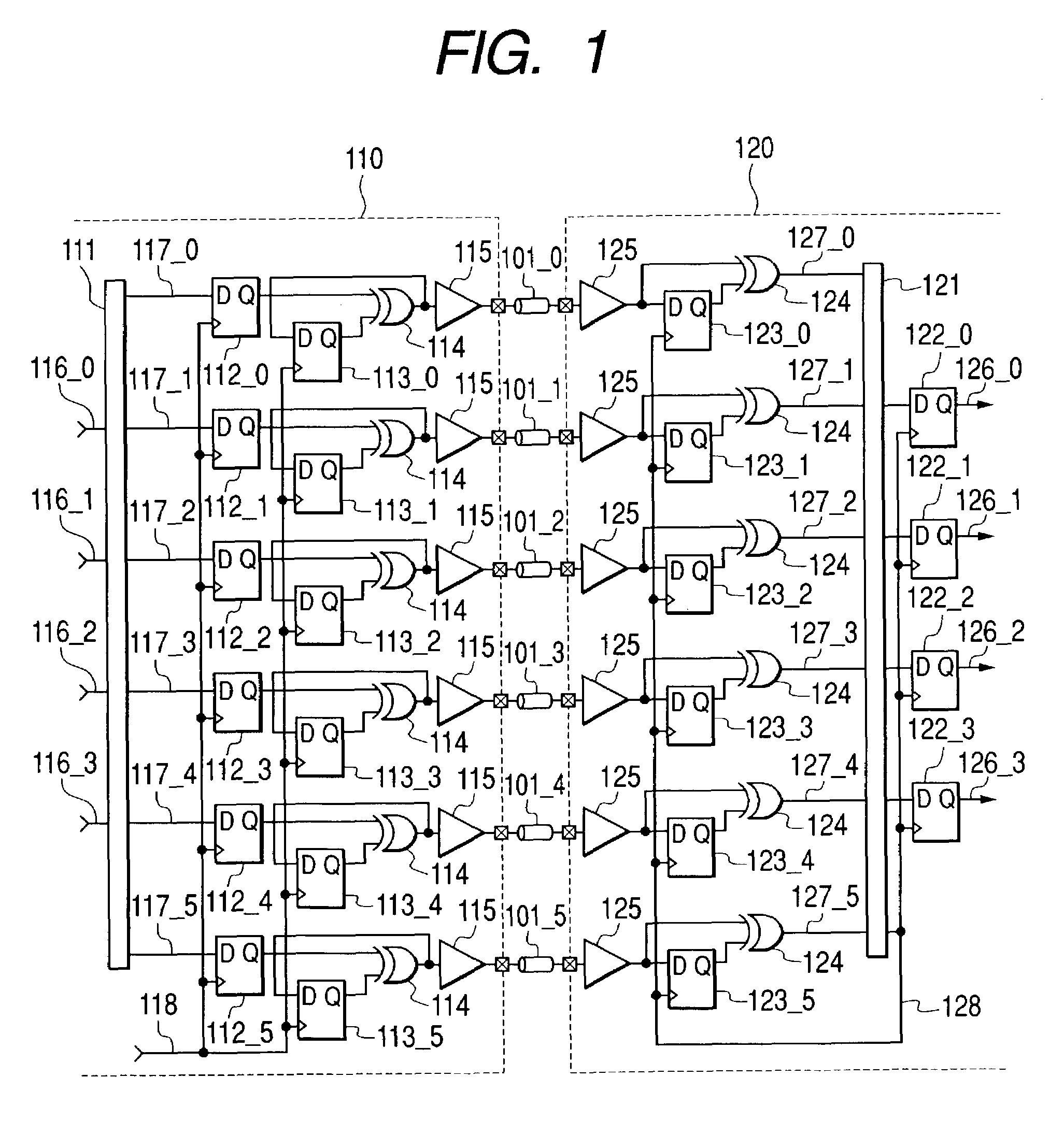
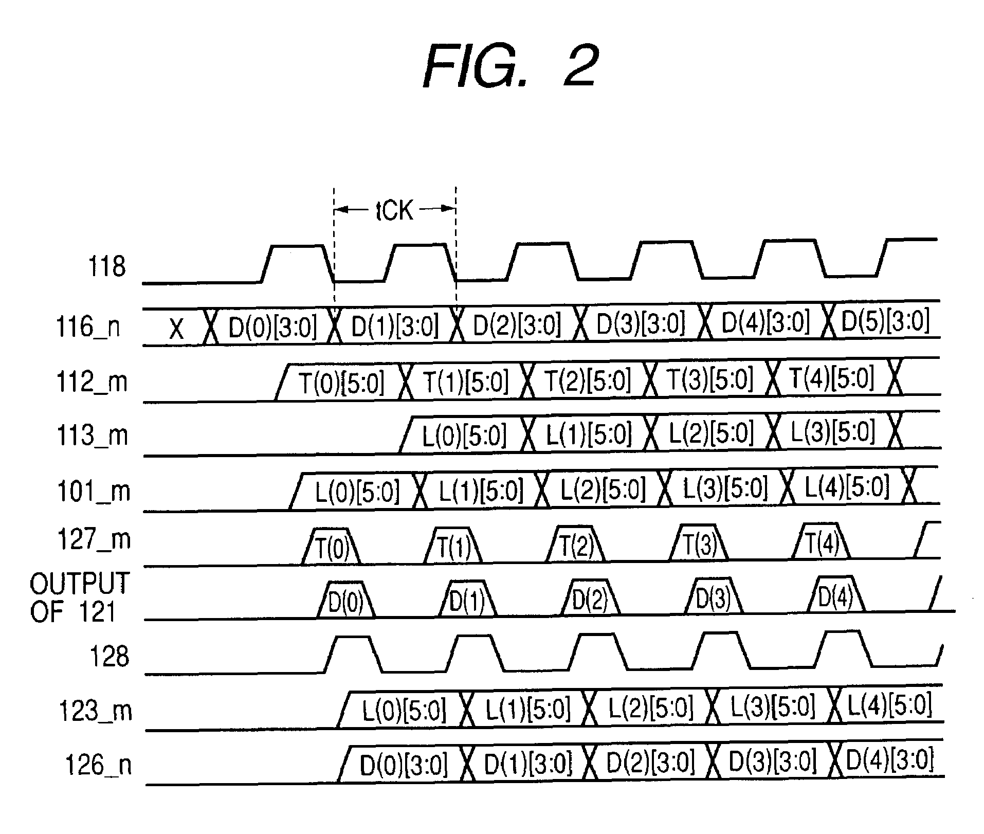
[0040]FIG. 1 is a block diagram showing an embodiment of a data communication device according to the invention. The schematic configuration of the data communication device of the embodiment is as follows. Reference numeral 110 denotes a transmission-side device, and reference numeral 120 indicates a reception-side device. Although not limited, each of the transmission-side device 110 and the reception-side device 120 is formed as a semiconductor chip. The two semiconductor chips 110 and 120 are connected to each other via transmission lines 110_0 to 110_5. Although not particularly limited, the transmission lines 110_0 to 110_5 are formed by printed wiring on a mounting board on which the transmission-side device 110 and the reception-side device 120 are mounted.

[0041]In the transmission-side device 110, terminals 116_0 to 116_3 (116_n) are data input terminals to which transmission data generated by a not-illustrated data processing circuit included in the transmission-side devic...


PUM


Abstract

The present invention provides a data communication method and a data communication device capable of performing high-speed data communication by using a parallel link and higher-speed data communication by reducing a timing skew. A data communication method includes: a step of encoding data of N bits (N being 2 or larger) to transmission data of M bits (M being 3 or larger) on a transmission side; a step of generating a transmission signal in which transition takes place in at least one level of any of the transmission data synchronously with a transmission clock and transmitting the transmission signal to a transmission line on the transmission side; a step of recognizing transition in the signal of M bits received via the transmission line and detecting the reception data of M bits synchronized with the transmission clock on a reception side; and a step of decoding the reception data of M bits to the data of N bits.

Description

BACKGROUND OF THE INVENTION[0001]The present invention relates to a data communication device and a technique effectively applied for a technique of data communication performed between, mainly, an MPU (Micro Processing Unit) and a main storage device or the like.[0002]Methods of performing data communication between integrated circuits are roughly divided into a parallel communication method (parallel link) using a plurality of transmission lines and transmitting data in parallel, and a serial communication method (serial link) using a single transmission line and transmitting data in series. Usually, the parallel link can simultaneously transmit plural data, so that a transmission / reception data amount per unit time is large. However, since it is necessary to suppress a skew of timings of the plural data, the parallel link is generally used, for example, in data communication between the semiconductor integrated circuits having a short transmission line. On the other hand, in the ...

Claims


Application Information

Patent Timeline
Patent Type & Authority Patents(United States)
IPC IPC(8): H04L7/00G06F13/16H04L25/14H04L25/49
CPCH04L25/14H04L25/4908H04L7/033
Inventor OKUDA, YUICHISAKATA, TAKESHISATO, TAKASHI
Owner RENESAS ELECTRONICS CORP
Why Eureka
Try Eureka