System and method for providing an integrated circuit having increased radiation hardness and reliability

a technology of applied in the field of integrated circuit manufacturing, can solve the problems of system reliability problems, space electronic systems at risk of not meeting their usable life expectancy, radiation damage to the structure and operation of integrated circuits, etc., and achieve the effect of increasing radiation hardness and reliability

Active Publication Date: 2008-02-12
NAT SEMICON CORP
View PDF6 Cites 3 Cited by
  • Summary
  • Abstract
  • Description
  • Claims
  • Application Information

AI Technical Summary

Benefits of technology

[0009]To address the above-discussed deficiencies of the prior art, it is a primary object of the present invention...

Problems solved by technology

Radiation is capable of damaging the structure and operation of integrated circuits.
Because of the ELDRS effect, many of space electronic systems are at risk of not meeting their usable life expectancy.
The ELDRS effect has therefore created a systems reliability problem that is due to ra...

Method used


Image

  • System and method for providing an integrated circuit having increased radiation hardness and reliability
  • System and method for providing an integrated circuit having increased radiation hardness and reliability
  • System and method for providing an integrated circuit having increased radiation hardness and reliability

Examples


Embodiment Construction

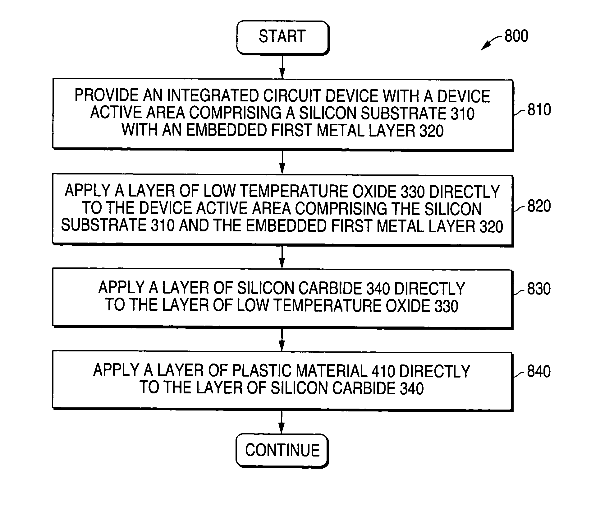
[0031]FIGS. 1 through 9 and the various embodiments used to describe the principles of the present invention in this patent document are by way of illustration only and should not be construed in any way to limit the scope of the invention. Those skilled in the art will understand that the principles of the present invention may be implemented in any type of suitably arranged integrated circuit.

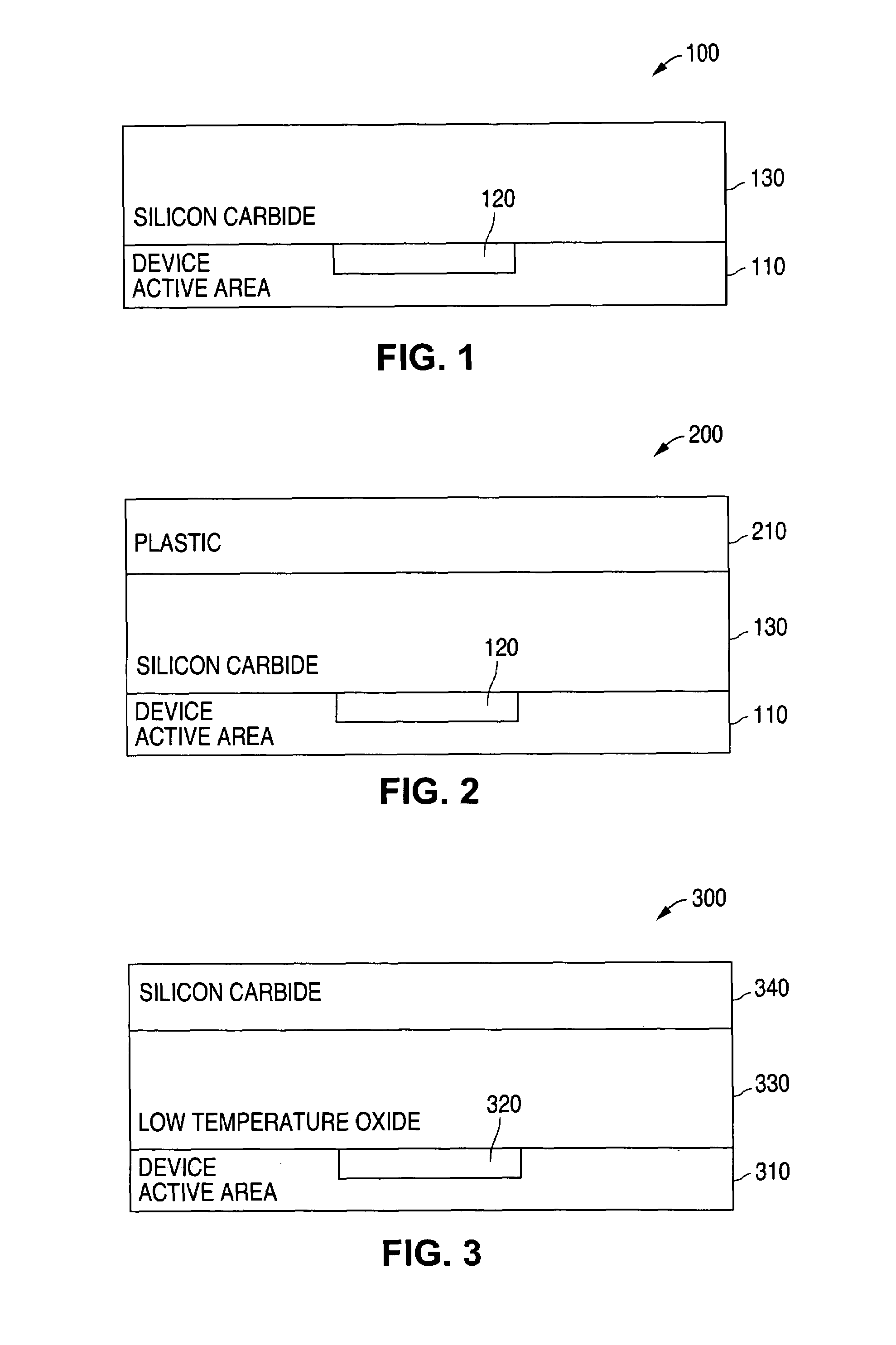
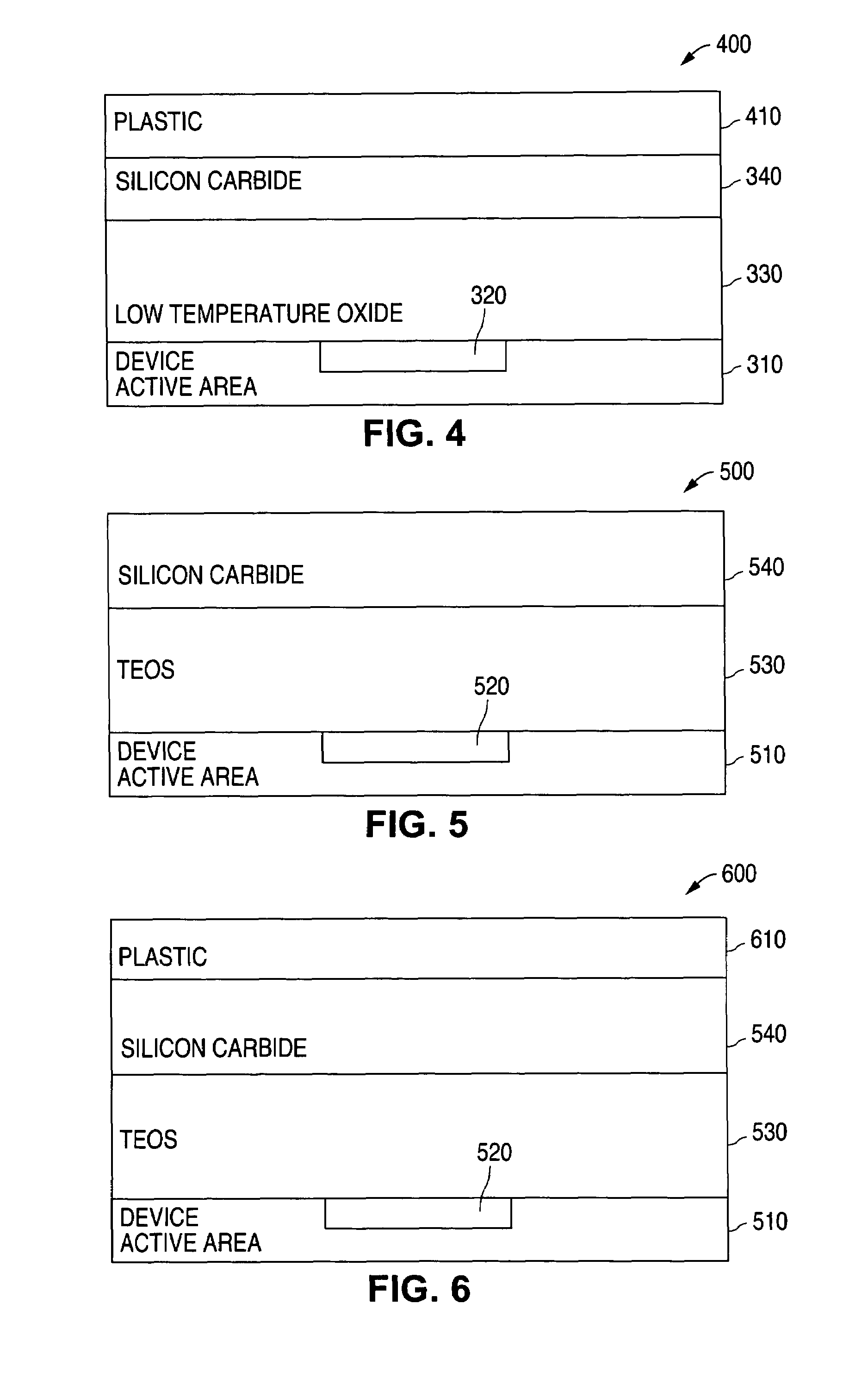
[0032]FIG. 1 illustrates a cross sectional schematic view of an advantageous embodiment of an integrated circuit 100 of the present invention. The integrated circuit 100 shown in FIG. 1 comprises a silicon substrate 110. Silicon substrate 110 may be located on a conventional underlying oxide layer (not shown) that is located on an underlying handle wafer (not shown). An exemplary first metal layer 120 is embedded within silicon substrate 110. Silicon substrate 110 and first metal layer 120 comprise the device active area of integrated circuit 100.

[0033]A layer of silicon carbide 130 is deposi...


PUM


Abstract

A system and method is disclosed for providing an integrated circuit that has increased radiation hardness and reliability. A device active area of an integrated circuit is provided and a layer of radiation resistant material is applied to the device active area of the integrated circuit. In one advantageous embodiment the radiation resistant material is silicon carbide. In another advantageous embodiment a passivation layer is placed between the device active area and the layer of radiation resistant material. The integrated circuit of the present invention exhibits minimal sensitivity to (1) enhanced low dose rate sensitivity (ELDRS) effects of radiation, and (2) pre-irradiation elevated temperature stress (PETS) effects of radiation.

Description

TECHNICAL FIELD OF THE INVENTION[0001]The present invention is generally directed to the manufacture of integrated circuits and, in particular, to a system and method for providing integrated circuits that have increased radiation hardness and reliability.BACKGROUND OF THE INVENTION[0002]Electronic equipment that is used in outer space (and in other radiation environments) contains integrated circuits that are exposed to radiation. Radiation is capable of damaging the structure and operation of integrated circuits. In particular, it is known that many bipolar linear integrated circuits exhibit enhanced low-dose-rate sensitivity (ELDRS) at low electric fields. In addition, many bipolar linear integrated circuits also exhibit pre-radiation elevated temperature stress (PETS) sensitivity. In the design and manufacture of integrated circuits it is desirable to eliminate (or at least minimize) the ELDRS and PETS effects in bipolar linear integrated circuits.[0003]It is known that the pass...

Claims


Application Information

Patent Timeline
IPC IPC(8): H01L21/26H01L29/00
CPCH01L24/29H01L2924/01013H01L2924/14H01L2924/3025H01L2224/29H01L2224/2919H01L2224/29298H01L2924/01033H01L2924/0665H01L2924/00H01L2924/00011H01L2924/0132H01L2924/01006H01L2924/01014H01L2924/00013H01L2224/29099H01L2224/29199H01L2224/29299H01L2224/2929
Inventor MAHER, MICHAEL C.
Owner NAT SEMICON CORP
Why Eureka
Try Eureka