Radiation hardened microcircuits

Inactive Publication Date: 2005-10-04
THE UNITED STATES OF AMERICA AS REPRESETNED BY THE SEC OF THE AIR FORCE
View PDF3 Cites 0 Cited by
  • Summary
  • Abstract
  • Description
  • Claims
  • Application Information

AI Technical Summary

Benefits of technology

[0009]According to one aspect of the present invention, a silicon-based semiconductor microcircuit is radiation hardened by replacing the standard finished circuit anneal process by heating the microcircuit in a vacuum furnace to remove any hydrogen in the microcircuit structure and annealing the microcircuit with deuterium containing forming gas. This process significantly increases the radiation hardness of the circuit while at the same time reducing hot carrier degradation and electrical stress induced leakage currents of individual circuit components.

Problems solved by technology

Failure of the device is usually observed when the hot electron induced degradation results in device channel mobility or threshold voltage shift outside a range of values considered acceptable.

Method used


Image

  • Radiation hardened microcircuits

Examples


Embodiment Construction

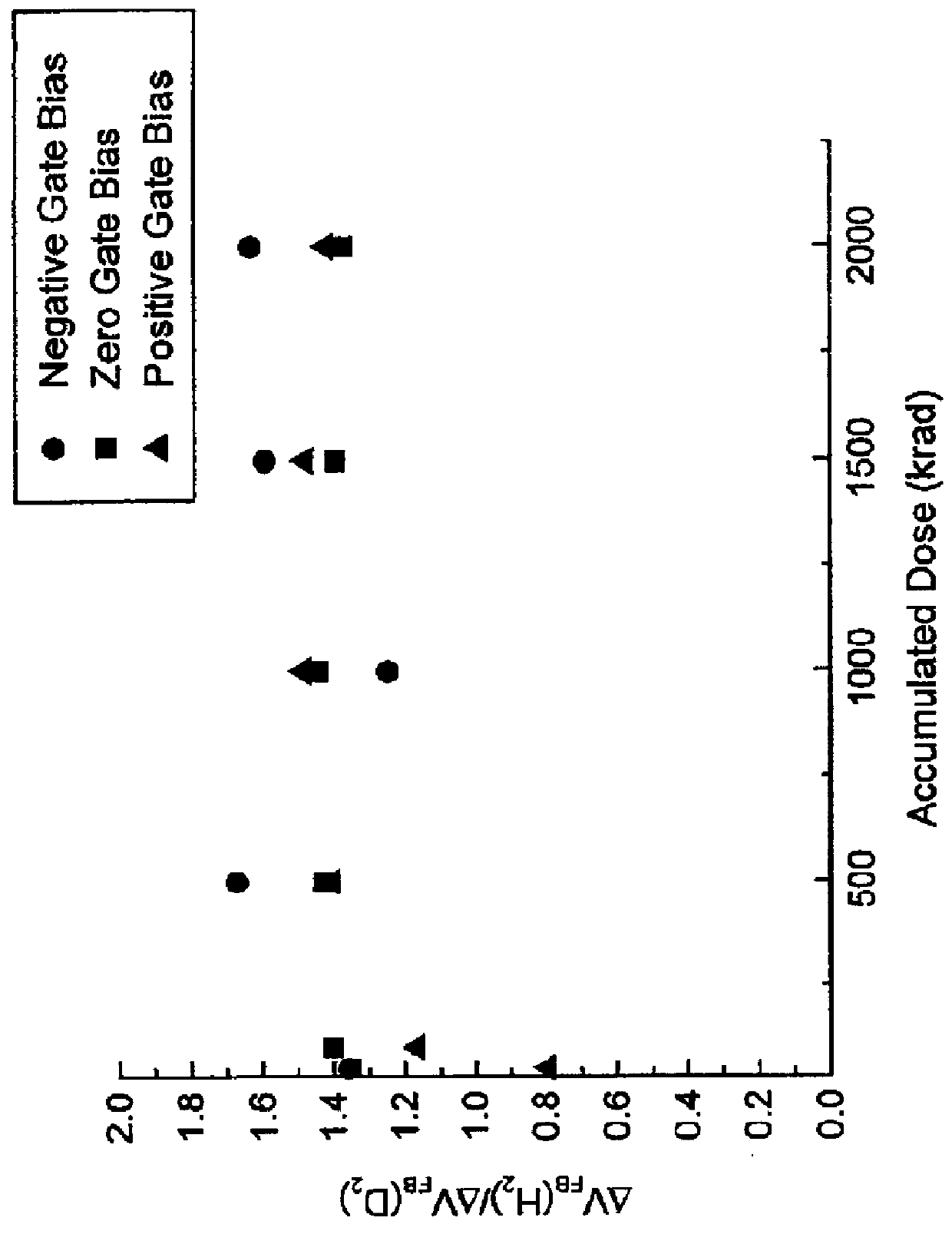
[0012]Typical silicon-based semiconductor circuits are made up of various devices, e.g., transistors, interconnect lines between the various devices, and isolating dielectrics separating the devices and interconnects from each other. Of these components, the isolating dielectrics are the most susceptible to damage from external radiation. The annealing process of the present invention significantly improves the radiation hardness of these circuits while at the same time reducing hot carrier degradation and electrical stress-induced leakage currents in the individual devices of which the circuit is partly comprised.

[0013]One aspect of the invention is the unique post-fabrication annealing process applied to the semiconductor circuit. First, the finished circuit is baked in a vacuum (−6 torr) for approximate one hour at about 500° C. to remove any hydrogen in the circuit resulting from the fabrication process. The temperature of this out-gassing anneal stage is chosen to enhance remov...


PUM


Abstract

A method of radiation hardening microcircuits including the steps of removing hydrogen from the microcircuit in a vacuum furnace and annealing in deuterium-containing forming gas.

Description

FEDERAL RESEARCH STATEMENT[0001][The condition under which this invention was made are such as to entitle the Government of the United States under paragraph I(a) of Executive Order 10096, as represented by the Secretary of the Air Force, to the entire right, title and interest therein including foreign rights.]BACKGROUND OF INVENTION[0002]The present invention is in the field of semiconductor device fabrication, and in particular, relates to the radiation hardening of microcircuits.[0003]In standard microelectronics technology one of the finally processes undergone is an anneal of the finished circuit in forming gas (a mixture of hydrogen and nitrogen or argon) at temperatures in the range 380° C. to 430° C. for periods of up to 30 minutes. Rapid thermal annealing has also been used. The primary objective of these anneals is to passivate the interface (dielectric / semiconductor) of the metal-oxide-semiconductor field effect transistors (MOSFETs) in order to enhance the carrier mobil...

Claims


Application Information

Patent Timeline
IPC IPC(8): H01L21/28H01L21/30H01L21/324H01L23/552
CPCH01L21/28185H01L21/28176H01L21/28194H01L21/28211H01L21/3003H01L21/324H01L23/552H01L2924/0002
Inventor DEVINE, RODERICK ANTHONY BLUNDENCHAVEZ, JOSEPH R.
Owner THE UNITED STATES OF AMERICA AS REPRESETNED BY THE SEC OF THE AIR FORCE
Why Eureka
Try Eureka