Method for manufacturing image-forming apparatus involving changing a polymer film into an electroconductive film

Inactive Publication Date: 2008-02-26
CANON KK
View PDF40 Cites 9 Cited by
  • Summary
  • Abstract
  • Description
  • Claims
  • Application Information

AI Technical Summary

Benefits of technology

[0019]An object of the present invention is to provide an electron-emitting

Problems solved by technology

In addition, since it is difficult to obtain adequate electron emission by means of the gap formed by the forming, there has been a technique in which carbons or carbon compounds are opposed with each other with a narrower gap portion within the gap formed by the forming, by effecting the above-mentioned activation processing or the processing for coating organic polymer film and for effecting energization.
Accordingly, the conventional devices arise the following two problems:1) When the fine particle film is used as the conduc

Method used


Image

  • Method for manufacturing image-forming apparatus involving changing a polymer film into an electroconductive film
  • Method for manufacturing image-forming apparatus involving changing a polymer film into an electroconductive film
  • Method for manufacturing image-forming apparatus involving changing a polymer film into an electroconductive film

Examples


embodiment 1

[Embodiment 1]

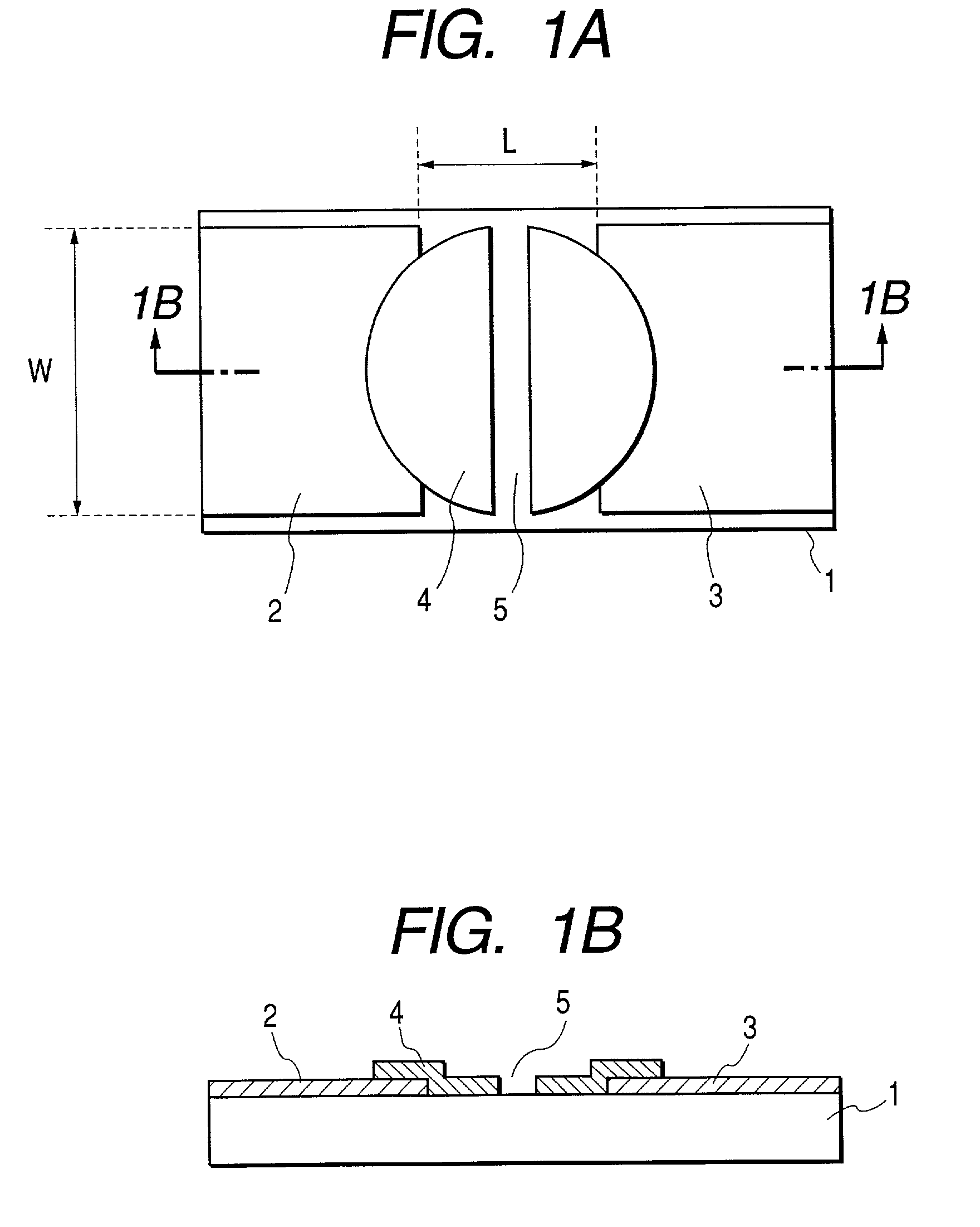
[0102]As the electron-emitting device according to an embodiment 1, the electron-emitting device of type shown in FIGS. 1A and 1B was formed by using a method similar to the manufacturing method shown in FIGS. 2A to 2C. Now, the method for manufacturing the electron-emitting device according to the embodiment 1 will be described with reference to FIGS. 1A and 1B and FIGS. 2A to 2C.

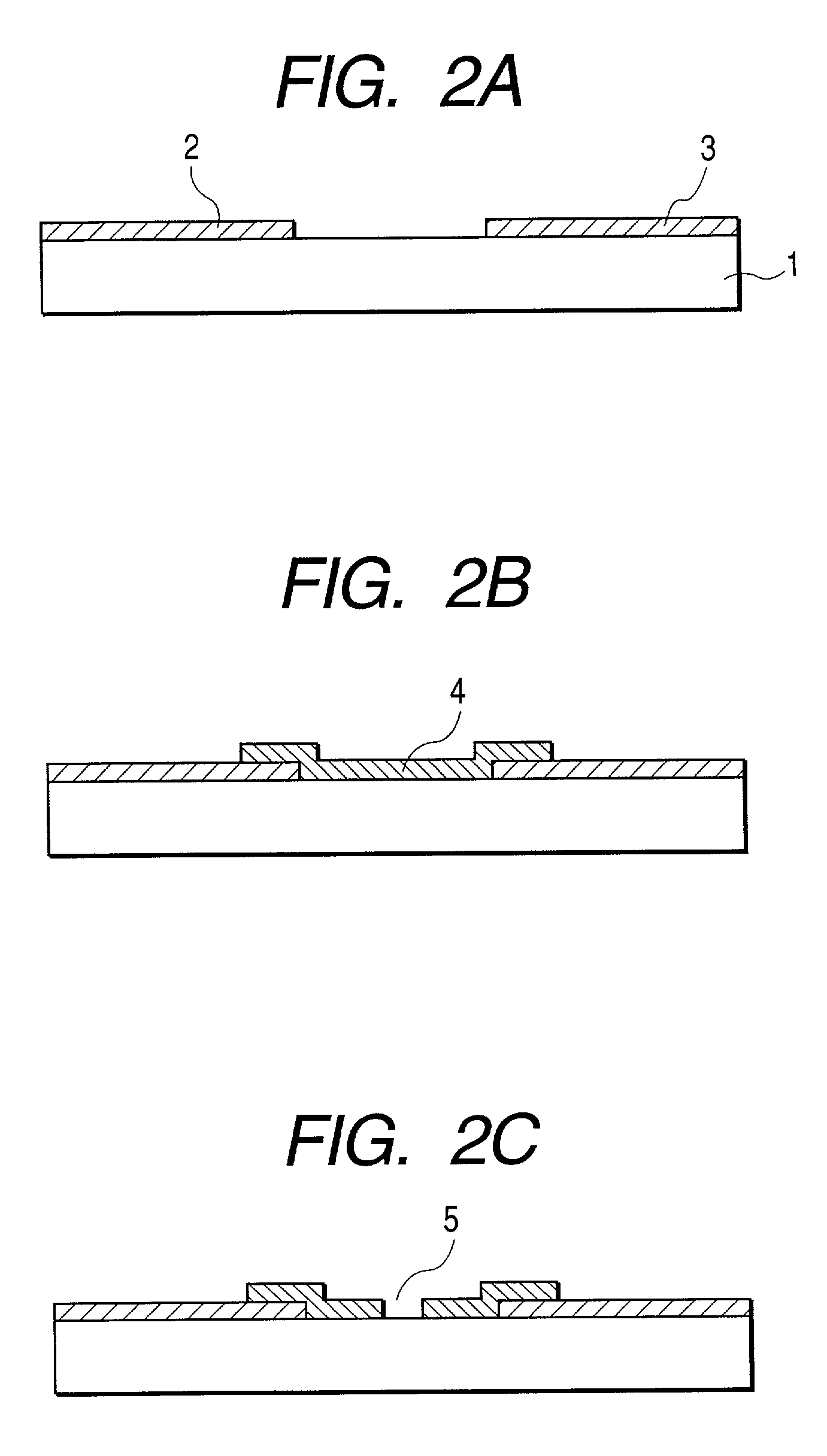
[0103]A quartz glass substrate was used as the substrate 1, and the substrate 1 was fully cleaned by using pure water, organic solvent and the like. Thereafter, the device electrodes 2, 3 made of platinum were formed on the substrate 1 (FIG. 2A). In this case, a distance L between the device electrodes was selected to 10 μm, a width of the device electrode was selected to 500 μm and a thickness of the device electrode was selected to 100 μm.

[0104]Then, polyamic acid solution (PIX-L110; manufactured by Hitachi Kasei Co., Ltd.) as precursor for aromatic polyimide and solution diluted by N-methy...

embodiment 2

[Embodiment 2]

[0113]The electron-emitting device according to an embodiment 2 fundamentally has a configuration similar to that of the electron-emitting device of the embodiment 1.

[0114]Similar to the embodiment 1, N-methyl pyrrolidone / n-butyl Cellosolve solution of 3% of polyphenylenen hydrazide as precursor for polyphenylene oxisadiazol was rotary-coated on the quartz glass substrate on which the device electrodes 2, 3 formed from platinum were formed, manufactured in this way by means of a spin-coater. Then, a temperature was increased up to 310° C. under vacuum to effect baking, thereby obtaining polyphenylene oxisadiazol film having a thickness of 30 nm.

[0115]The polyphenylene oxisadiazol film was patterned to form a square configuration of 300 μm×300 μm straddling between the device electrodes 2 and 3 by a photolithography technique, thereby forming the polymer film having a desired configuration.

[0116]Then, after the electron beam was illuminated on the entire surface of the ...

embodiment 3

[Embodiment 3]

[0120]The electron-emitting device according to an embodiment 3 fundamentally has a configuration similar to that of the electron-emitting devices of the embodiments 1 and 2.

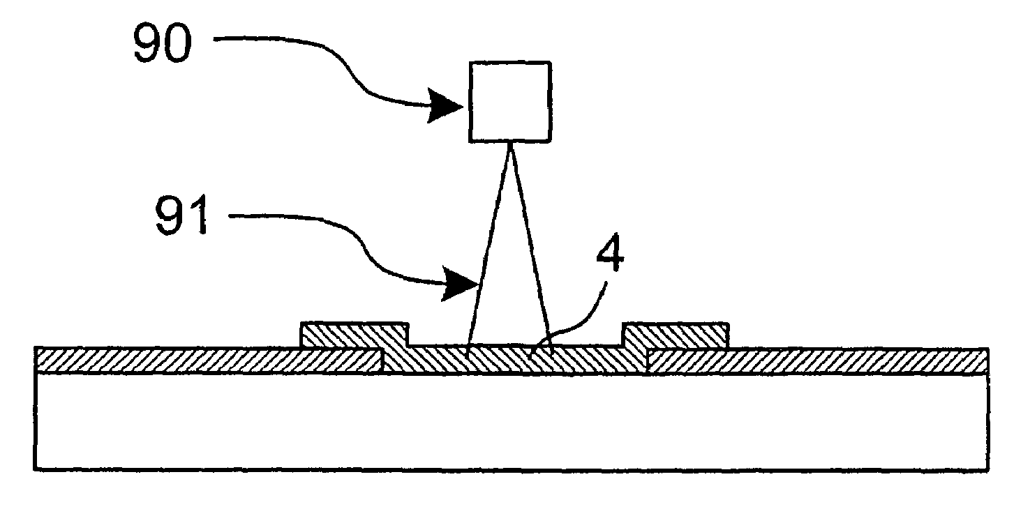
[0121]Similar to the embodiment 1, the quartz glass substrate 1 on which the device electrodes 2, 3 comprised of platinum and the polymer film 4 comprised of polyimide film were formed was set in a vacuum container to which an electronic gun was mounted and adequate air discharge was performed. Thereafter, bipolar rectangular pulses having voltage of 25 V, pulse width of 1 msec and pulse interval of 10 msec were applied between the device electrodes 2 and 3 while illuminating electron beam having acceleration voltage Vac of 7 kV and current density ρ of 0.1 mA / mm2 onto the whole surface of the polymer film 4. In this case, the current flowing between the device electrodes 2 and 3 was gradually increased, and, after the current was increased up to about 2.5 mA, since the current was suddenly decreas...


PUM


Abstract

The present invention provides a method for manufacturing an electron-emitting device, comprising a step for forming a polymer film between a pair of electrodes formed on a substrate, a step for giving conductivity to the polymer film by heating, and a step for providing potential difference between the pair of electrodes.

Description

BACKGROUND OF THE INVENTION[0001]1. Field of the Invention[0002]The present invention relates to an electron-emitting device, an electron beam in which a number of electron-emitting elements are arranged, and a method for forming an image-forming apparatus such as a display constituted by using such an electron source. More specifically, the present invention relates to a method for manufacturing an electron emitting-device comprising a substrate, a pair of electrodes formed on the substrate, and a film having a narrow gap and connected between the electrodes.[0003]2. Related Background Art[0004]Conventionally, as electron-emitting devices, two kinds of devices, i.e., a heat electron-emitting device and cold cathode electron-emitting device are known. The cold cathode electron-emitting device is divided into electrical field emitting type, metal / insulator / metal type and surface conduction electron-emitting type.[0005]A construction and manufacturing method for the surface conduction...

Claims


Application Information

Patent Timeline
IPC IPC(8): H01J9/04H01J9/00H01J9/12H01J9/24H01J9/44H01J9/02H01J1/30
CPCH01J9/027H01J1/30
Inventor IWAKI, TAKASHIMIZUNO, HIRONOBUSHIBATA, MASAAKIMIYAZAKI, KAZUYA
Owner CANON KK
Why Eureka
Try Eureka