Semiconductor memory device allowing high-speed data reading

a memory device and semiconductor technology, applied in the direction of information storage, static storage, digital storage, etc., can solve the problems of large load, inability to implement high-speed reading, and increase the load of bit lines, so as to reduce the load of an internal data bus and high-speed data reading

Active Publication Date: 2008-03-04
RENESAS ELECTRONICS CORP
View PDF13 Cites 1 Cited by
  • Summary
  • Abstract
  • Description
  • Claims
  • Application Information

AI Technical Summary

Benefits of technology

[0022]An object of the present invention is to provide a semiconductor memory device enabling high-speed data reading by reducing a load of an internal data bus connected to a sense amplifier.
[0023]Another object of the present invention is to provide a static semiconductor memory device which can transfer internal read data at a high speed without increasing a chip layout area.
[0028]Each memory block is divided into subarrays for which data lines are provided, respectively, and the data line for a selected subarray is coupled to the sense node of a sense amplifier. Therefore, only a capacitance of a column selection gate (arranged corresponding to each bit line pair) of a column selection circuit of a corresponding subarray and a bit line load are connected to the data line, which can reduce a load of the data line of the sense amplifier and can provide a similar effect of reduction of a bit line load in a bit line division structure on an internal data line, to allow implementation of high-speed data reading even when the number of memory cell rows is increased.
[0029]In addition, by arranging a plurality of memory blocks for one bit of data, dividing each memory block into first and second subarrays and arranging a sense read circuit and an internal write circuit between the first and second subarrays, a length of the bit line can be decreased even when the number of memory cells is increased and, correspondingly, the bit line load is reduced while a load of the internal data line is similarly reduced to allow implementation of high-speed writing / reading. Furthermore, only sense read circuits and internal write circuits corresponding in number to the memory blocks are connected to the global data bus, which in turn has a small load and can transfer internal data at a high speed.

Problems solved by technology

In addition, a main amplifier for amplifying the internal read data and a write driver for writing data are further connected to the common data line, and therefore the load becomes large.
Therefore, since the memory plane is not divided in a bit line direction in this construction, when the number of memory cells is increased in the bit line direction, a bit line load is accordingly increased and therefore high-speed reading cannot be implemented.
When the number of the memory cells is further increased, however, the load of the bit line is accordingly increased and thus high-speed writing / reading of data cannot be implemented.
Although prior art document 4 describes a divided-in-two structure for the bit line, a problem of increase in bit line load when the number of the memory cells is further increased in the bit line direction is not considered.

Method used


Image

  • Semiconductor memory device allowing high-speed data reading
  • Semiconductor memory device allowing high-speed data reading
  • Semiconductor memory device allowing high-speed data reading

Examples


first embodiment

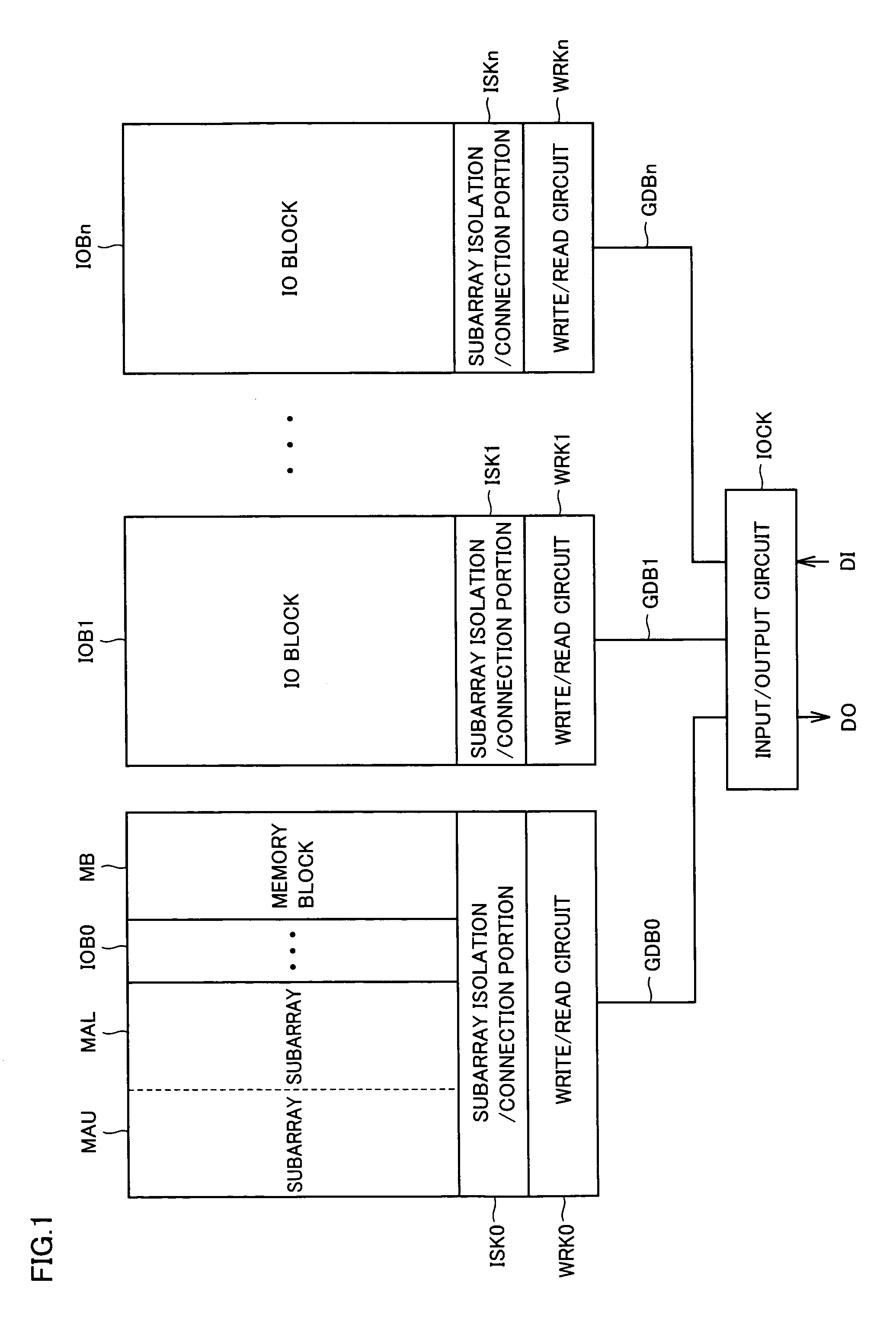
[0053]FIG. 1 is a conceptual diagram of a construction of a main portion of a semiconductor memory device according to a first embodiment of the present invention. In FIG. 1, a memory array is divided into a plurality of IO blocks IOB0-IOBn. Each of IO blocks IOB0-IOBn corresponds to one bit of external input data DI and external output data DO. IO blocks IOB0-IOBn concurrently input and output data.

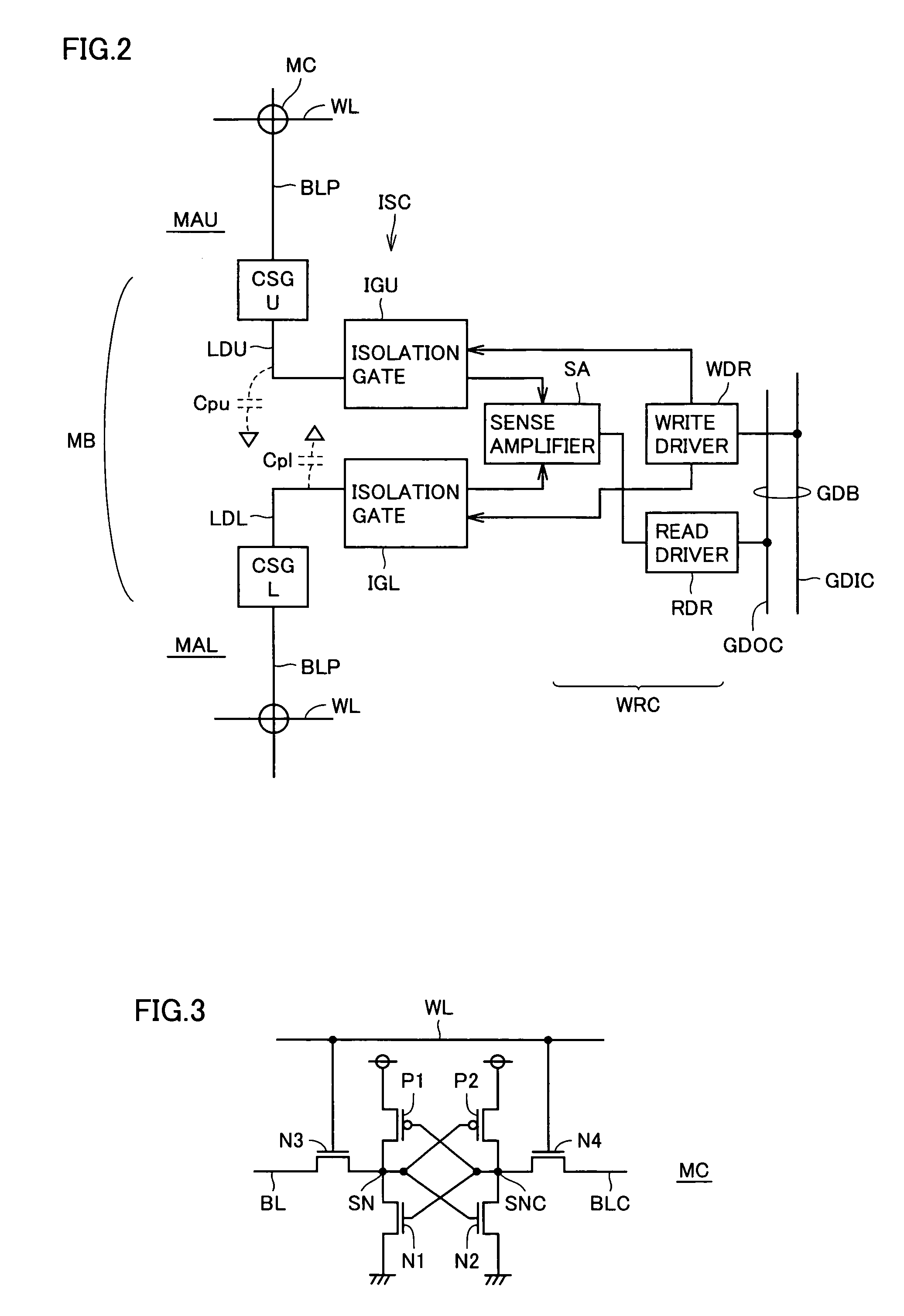
[0054]Each of IO blocks IOB0-IOBn is divided into a plurality of memory blocks MBs. Memory block MB in IO block IOB0 is representatively shown in FIG. 1. Memory block MB is further divided into subarrays MAU and MAL. One memory block MB is selected in each of IO blocks IOB0-IOBn, and one of subarrays MAU and MAL in a selected memory block is further selected.

[0055]IO blocks IOB0-IOBn, respectively, include write / read circuits WRK0-WRKn for writing / reading internal data and subarray isolation / connection portions ISK0-ISKn for performing isolation / connection of write / read circuits WRK0-WRK...

second embodiment

[0151]FIG. 14 schematically shows a construction of column circuit YC of a semiconductor memory device according to a second embodiment of the present invention. Column circuit YC shown in FIG. 14 is different in construction from column circuit YC shown in FIG. 5 in the following points. Specifically, data line precharge circuit DPCG is provided for local data lines DU and DCU. The data line precharge circuit is not arranged for local data lines DL and DCL for subarray MAL.

[0152]In addition, subarray specifying signals BSCL and BSCU are generated in synchronization with internal clock signal ICLK. The other portions of the construction of column circuit YC shown in FIG. 14 are the same as those of column circuit YC shown in FIG. 5, and corresponding portions are indicated with the same reference characters and detailed descriptions thereof will not be repeated.

[0153]FIG. 15 is a signal waveform diagram representing an operation in data reading of column circuit YC shown in FIG. 14....

third embodiment

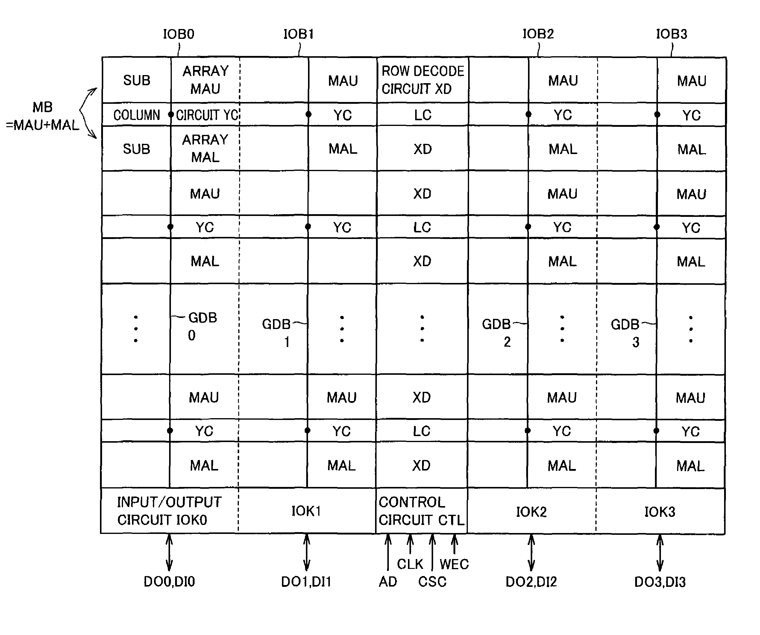
[0165]FIG. 17 schematically shows a construction of a main portion of a semiconductor memory device according to a third embodiment of the present invention. The semiconductor memory device in FIG. 17 inputs / outputs data of 4 bits, by way of example. Data bits DO0-DO3 indicate output data bits and data bits DI0-DI3 indicate input data bits. IO blocks IOB0-IOB3 are provided corresponding to respective inputs / output bits DO0, DI0-DO3, DI3. Data of 1 bit is input and output at each of IO blocks IOB0-IOB3.

[0166]Similarly as in the first and second embodiments, each of IO blocks IOB0-IOB3 is divided into a plurality of memory blocks MBs, and each memory block MB is divided into upper subarray MAU and lower subarray MAL. Column circuit YC is arranged between subarrays MAU and MAL of memory block MB. Column circuit YC includes a sense read circuit (the sense amplifier and the read driver), an internal write circuit (the write driver), an isolation / connection gate (the connection control ci...


PUM


Abstract

Each of a plurality of memory blocks arranged for 1 bit data is divided into two subarrays. A separate local data line is provided for each subarray and coupled to a sense amplifier via an isolation gate. A memory cell is selected in a selected subarray of a selected memory block, and a bit line of the selected memory cell is coupled to a corresponding local data line. Only a local data line of the selected subarray is coupled to the sense amplifier to perform a sense operation, and a global read data line is driven via a read driver in accordance with an output signal of the sense amplifier. A load of a sense node of the sense amplifier in a semiconductor memory device is reduced to implement high-speed reading of internal data.

Description

BACKGROUND OF THE INVENTION[0001]1. Field of the Invention[0002]The present invention relates to a semiconductor memory device, in particular, to a static semiconductor memory device (SRAM: Static Random Access Memory). More specifically, the present invention relates to a construction of an internal data read and data transfer portion of the SRAM.[0003]2. Description of the Background Art[0004]An SRAM has a memory cell formed with a latch circuit, and complementary data are kept at storage nodes inside the memory cell. Therefore, an SRAM cell can stably store data while power is supplied, and refreshing of stored data is not required in contrast to a construction of a DRAM (Dynamic Random Access Memory), which in turn stores information according to electric charges of a capacitor. Thus, the SRAM is controlled more easily than the DRAM, and is widely used in various processing systems.[0005]In addition, since memory cell data can be accurately read from the SRAM even when a row and...

Claims


Application Information

Patent Timeline
Patent Type & Authority Patents(United States)
IPC IPC(8): G11C8/00G11C15/02G11C7/06
CPCG11C7/1051G11C7/1066G11C7/1069G11C7/1078G11C7/1096G11C11/413G11C2207/005
Inventor MORISHIMA, CHIKAYOSHI
Owner RENESAS ELECTRONICS CORP
Why Eureka
Try Eureka