Integrated circuit incorporating wire bond inductance

a wire bond and integrated circuit technology, applied in the field of electromechanical devices, can solve the problems of small inductance generation, unsuitable application techniques, and unpredictable inductan

Inactive Publication Date: 2008-03-11
ZARBANA DIGITAL FUND
View PDF20 Cites 21 Cited by
  • Summary
  • Abstract
  • Description
  • Claims
  • Application Information

AI Technical Summary

Benefits of technology

[0015]The advantage of the present invention are readily apparent. Instead of being a problem which a designer must try to overcome the inductance inherent in wire bonds can be utilized as an integral component of a functional circuit on the chip.
are readily apparent. Instead of being a problem which a designer must try to overcome the inductance inherent in wire bonds can be utilized as an integral component of a functional circuit on the chip.

Problems solved by technology

Although greater I / O density can be achieved using this packaging technique, problems such as controlling heat dissipation are prevalent making this technique unsuitable for some applications.
As will be appreciated by those in the art, a problem with wire bonds for high frequency circuits is that they also generate a small amount of inductance (e.g. 1 nanoHenry / millimetre of length).
In the case of a wire bond, the inductance is often unpredictable because, typically, the exact length of the wire is inconsistent, as well as its location and termination point on either the chip or carrier pad.
The inconsistencies are largely a result of imprecise manufacturing techniques.
As a result, this heretofore undesirable property of wire bonds has presented problems to integrated circuit designers who have tried to design around the inductance produced by wire bonds.
In either case, recognized problems are created for the circuit designer.

Method used


Image

  • Integrated circuit incorporating wire bond inductance
  • Integrated circuit incorporating wire bond inductance
  • Integrated circuit incorporating wire bond inductance

Examples


Embodiment Construction

[0023]In essence, the invention takes advantage of a physical property of a wire bond which had previously been considered undesirable. As a result of the advancement of manufacturing techniques the bond wires and ribbons can be made of a consistent length and bonded to electrical contacts on the package with sufficient precision to ensure that the inductance associated with the wire bond is predictable and therefore useable.

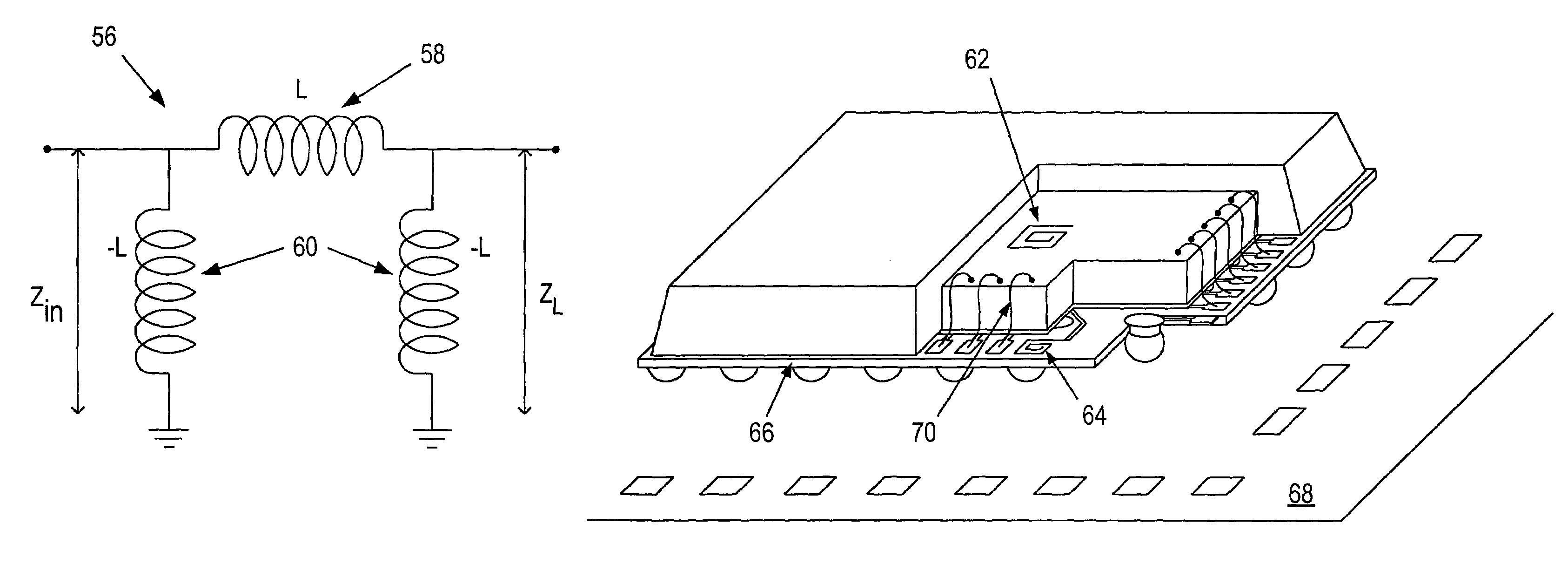
[0024]FIG. 5 depicts a lumped element impedance inverter 56. As those skilled in the art will appreciate, impedance is the total opposition to the flow of alternating current in a circuit that contains resistance and reactance. In the case of pure inductance, inductive reactance is the total opposition to the flow of current through it. An impedance inverter serves to transform a low output impedance to a high output impedance. As shown in the figure, the lumped element impedance inverter 56 consists of a series (positive) inductor 58 (also labelled “L”) and two...


PUM


Abstract

The invention relates to the field of electronics, more particularly to the wire bonds incorporated into an integrated circuit package such as a quad flat pack, a ball grid array or hybrid style module. The present invention takes the normally undesirable wire bond inductance and uses it in an operational circuit where positive inductance is required. The circuit in which the wire bond inductance is used is located primarily in the integrated circuit die housed in the integrated circuit package, but may also include off-die components. In one example, a wire bond is used as the required series inductance in a discrete circuit impedance inverter which consists of two shunt-to-ground negative inductances and one series positive inductance. One of the negative inductances is located on-die, while the other is located off-die.

Description

BACKGROUND OF THE INVENTION[0001]1. Field of the Invention[0002]The invention relates to the field of electronics, more particularly to the wire bonds incorporated into an integrated circuit package.[0003]2. Description of the Related Prior Art[0004]As will be understood by those skilled in the art, an integrated circuit (IC), sometimes called a chip or microchip is a semiconductor material on which thousands of tiny resistors, capacitors, and transistors are fabricated in a particular configuration to perform a desired electronic function. For example, a chip can function as an amplifier, oscillator, timer, counter, computer memory or microprocessor. A particular chip is categorized as either digital or analogue, depending on its intended application.[0005]In the manufacture of a chip a semiconductor wafer (typically 300 mm diameter for silicon) is doped to enhance its electron transfer properties and then etched to provide the desired circuitry. The resulting wafer is diced using ...

Claims


Application Information

Patent Timeline
Patent Type & Authority Patents(United States)
IPC IPC(8): H01L21/44H01L21/50H01L23/31H01L23/522H01L23/66
CPCH01L23/5227H01L23/66H01L23/645H01L23/3128H01L2223/6611H01L2224/16H01L2224/45014H01L2224/45144H01L2224/48091H01L2924/01014H01L2924/0105H01L2924/01078H01L2924/01079H01L2924/14H01L2924/15173H01L2924/15311H01L2924/19041H01L2924/30107H01L2924/3011H01L2924/00014H01L24/45H01L24/48H01L2924/00H01L2224/48227H01L24/49H01L2224/49171H01L2224/49175H01L2924/181H01L2924/00012H01L2224/0401H01L2924/206
Inventor WIGHT, JAMES STUARTGRUNDLINGH, JOHAN M.
Owner ZARBANA DIGITAL FUND
Why Eureka
Try Eureka