Light emitting device having organic light emitting material with mixed layer

a light emitting device and organic technology, applied in the direction of luminescnet screens, discharge tubes, instruments, etc., can solve the problems of difficult control of evaporation amount and small amount of pigment used in doping

Inactive Publication Date: 2008-03-11
SEMICON ENERGY LAB CO LTD
View PDF75 Cites 56 Cited by
  • Summary
  • Abstract
  • Description
  • Claims
  • Application Information

AI Technical Summary

Benefits of technology

[0078]The first mixed region and the second mixed region that are employed by the organic light emitting element of the present invention described above may have concentration gradient as shown

Problems solved by technology

A demerit of the method is that the amount of pigment used in doping is usually very small (less than 1 wt % in some cases) and contr

Method used


Image

  • Light emitting device having organic light emitting material with mixed layer
  • Light emitting device having organic light emitting material with mixed layer
  • Light emitting device having organic light emitting material with mixed layer

Examples


embodiment mode 1

[Embodiment Mode 1]

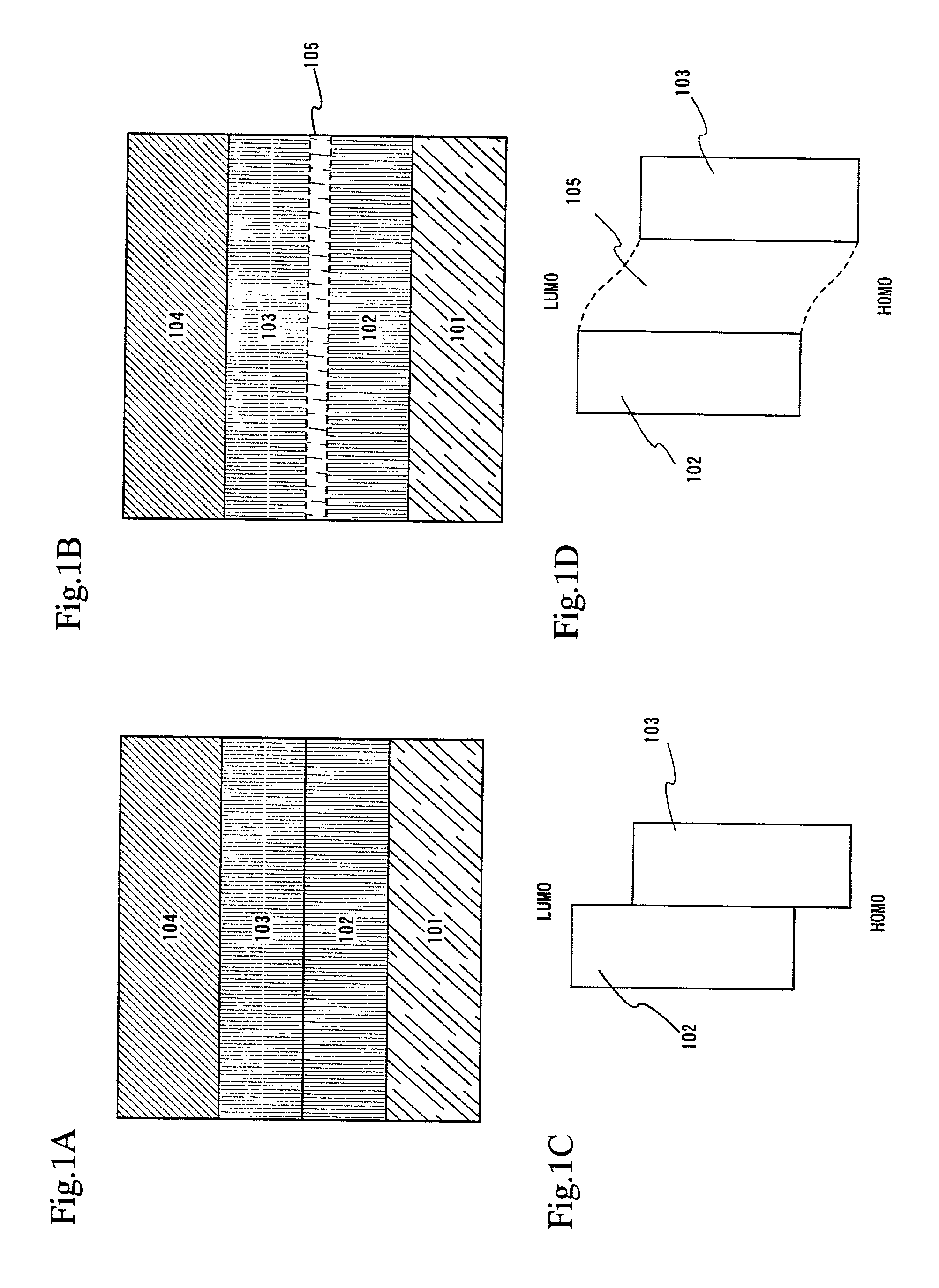
[0134]Embodiment Mode 1 describes a case of forming mixed layers at interfaces of organic compound layers with a light emitting layer in an organic light emitting element that has an organic compound layer 403 between an anode 401 and a cathode 402 as shown in FIG. 4.

[0135]In this embodiment mode, the organic compound layer 403 has a laminate structure of a plurality of organic compound layers. Specifically, a hole injecting layer 404 for improving injection of holes from the anode is formed on the anode 401, and a hole transporting layer 405 for improving transportation of the injected holes is formed on the hole injection layer 404.

[0136]A mixed layer (1) 407 is formed by coevaporation using the material that constitutes the hole transporting layer 405 and the material that constitutes a light emitting layer 406. The coevaporation is carried out in the manner described above. At this point, the mixed layer (1) 407 may have concentration gradient.

[0137]By providi...

embodiment mode 2

[Embodiment Mode 2]

[0142]Embodiment Mode 2 gives a description on a case of manufacturing an organic light emitting element with an element structure different from the one shown in Embodiment Mode 1.

[0143]The description given in Embodiment Mode 2 is a case in which mixed layers are formed at interfaces of organic compound layer with a laminate structure when an organic light emitting element is a triplet light emission element.

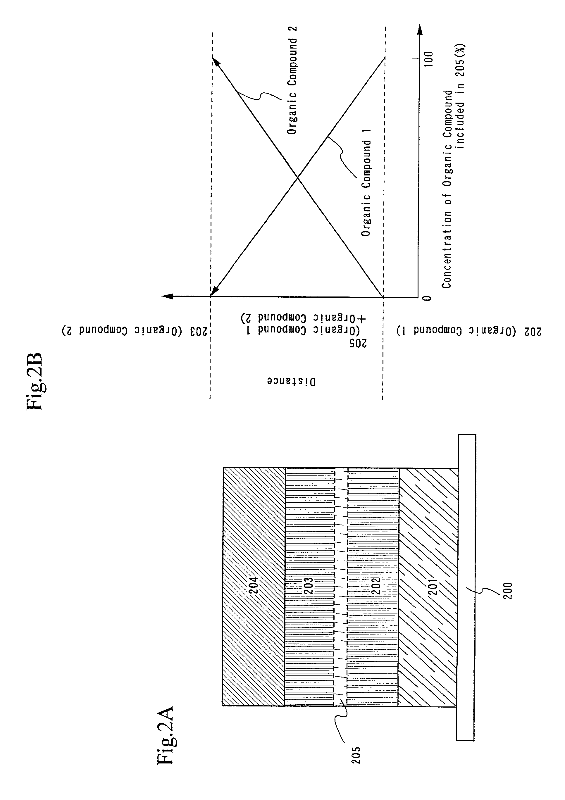
[0144]In Embodiment Mode 2, a laminate organic compound layer 503 with a plurality of organic compound layers is formed between an anode 501 and a cathode 502 as shown in FIG. 5. Specifically, a hole injection layer 504 for improving injection of holes from the anode 501 is formed on the anode 501, and a hole transporting layer 505 for improving transportation of the injected holes is formed on the hole injection layer 504.

[0145]A mixed layer (1) 507 is formed by coevaporation using the material that constitutes the hole transporting layer 505 and the materi...

embodiment mode 3

[Embodiment Mode 3]

[0153]Embodiment Mode 3 gives a description with reference to FIG. 6 in a case of manufacturing an organic light emitting element with an element structure different from the one shown in Embodiment Mode 1 or Embodiment Mode 2.

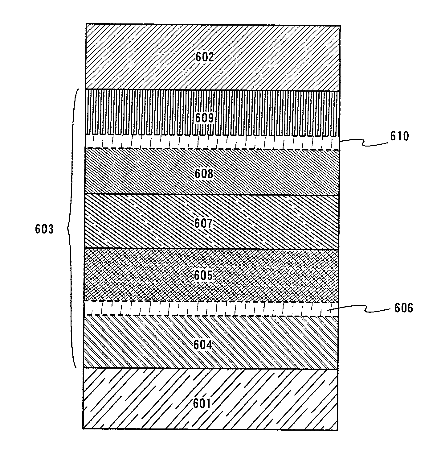
[0154]The description given in Embodiment Mode 3 is a case in which an organic light emitting element has an organic compound layer 603 between an anode 601 and a cathode 602 and mixed layers are formed at interfaces between injecting layers and transporting layers in the organic compound layer.

[0155]In Embodiment Mode 3, the organic compound layer 603 has a structure in which a plurality of organic compound layers are laminated. Specifically, a hole injecting layer 604 for improving injection of holes from the anode 601 is formed on the anode 601.

[0156]In this embodiment mode, a mixed layer (1) 606 is formed here by coevaporation using the material that constitutes the hole injection layer 604 and the material that constitutes a hole transp...


PUM


Abstract

A light emitting device is provided which has a structure for lowering energy barriers at interfaces between layers of a laminate organic compound layer. A mixed layer (105) composed of a material that constitutes an organic compound layer (1) (102) and a material that constitutes an organic compound layer (2) (103) is formed at the interface between the organic compound layer (1) (102) and the organic compound layer (2) (103). The energy barrier formed between the organic compound layer (1) (102) and the organic compound layer (2) (103) thus can be lowered.

Description

BACKGROUND OF THE INVENTION[0001]1. Field of the Invention[0002]The present invention relates to a light emitting device using an organic light emitting element with a film containing an organic compound that emits light with application of electric field (hereinafter referred to as organic compound layer), as well as an anode and a cathode. Specifically, the present invention relates to a light emitting device using an organic light emitting element with lower drive voltage than before and longer lifetime. The term light emitting device in this specification refers to an image display device or a light emitting device that employs as a light emitting element an organic light emitting element. Also included in the definition of the light emitting device are a module in which a connector, such as an anisotropic conductive film (FPC: flexible printed circuit), a TAB (tape automated bonding) tape, or a TCP (tape carrier package), is attached to an organic light emitting element, a modu...

Claims


Application Information

Patent Timeline
IPC IPC(8): H05B33/02H01L51/50G09F9/30H01L27/32H05B33/10H05B33/12H05B33/14H05B33/22
CPCH01L51/5012H01L51/5008H01L51/5096H01L51/5072H01L51/0085H01L51/5016H01L51/5056H01L51/0081Y10S428/917Y02E10/549H10K85/324H10K85/342H10K30/865H10K50/18H10K50/11H10K2101/10H10K50/15H10K50/16H05B33/22H10K77/10
Inventor SEO, SATOSHIYAMAZAKI, SHUNPEI
Owner SEMICON ENERGY LAB CO LTD
Why Eureka
Try Eureka