Apparatus and methods for encapsulating microelectromechanical (MEM) devices on a wafer scale

a technology of microelectromechanical devices and encapsulation methods, which is applied in the direction of forming microstructural systems, semiconductor devices, and semiconductor/solid-state device details, etc., can solve the problems of mem device impairment risk, total product the cost of mem devices, so as to reduce the pressure

Inactive Publication Date: 2008-03-18
IBM CORP
View PDF9 Cites 82 Cited by
  • Summary
  • Abstract
  • Description
  • Claims
  • Application Information

AI Technical Summary

Benefits of technology

[0010]Exemplary embodiments of the invention generally include apparatus and methods for providing wafer-scale encapsulation of microelectromechanical (MEM) devices (e.g., resonators, filters) to protect the MEMs from the ambient and to provide either a controlled ambient or a reduced pressure. In particular, exemplary embodiments of the invention include methods for wafer-scale encapsulation of MEM devices, which enable wafer-scale encapsulation of MEM devices under desired ambient conditions that are not determined by the deposition conditions of a sealing process in which MEM release via holes are sealed or pinched-off (e.g., pressures less than a few mT are possible), and which prevent sealing material from being inadvertently deposited on the MEM device during the sealing process.

Problems solved by technology

A significant portion of the cost of MEM devices can be in the packaging, which can account for more than half of the total product cost for MEM devices.
However, when an MEM device is integrated with an integrated circuit, the above methods are not compatible with designs intended for flip-chip packaging (i.e. C4 mini solder balls) and assume that the MEM resonator or filter is exposed on the top surface of the chip.
This approach offers a simple low cost means of encapsulation but with some risk of MEM device impairment by undesired deposition of material on the active device during pinch-off processing.
This method is also limited to pressures of a few Torr or more in the sealed structure (i.e. the pressure at which the plasma deposition takes place) if a PECVD or CVD technique are used to perform the sealing operation.
Again, with such method, the ambient conditions of the device are determined by the deposition conditions of the sealing process used and, the sealing material can be inadvertently deposited on the active device.
As noted above, a disadvantage of these methods of sealing the access holes is that the ambient conditions of the device are determined by the deposition conditions of the sealing process used.
Additionally, any MEM component exposed to the evaporative flux will receive a significant deposition of material that can alter the performance of the MEM device.
For example, adding mass to a micro mechanical resonator (or beam) will change the operational frequency of the resonator or cause stress related distortions of the beam.
By way of further example, an MEM switch device could be rendered inoperative if coatings get onto the switch contact and cause shorts or opens.
The drawbacks of these techniques are the high pressure they would seal in the cavity and because they are generally performed at high temperatures (>200 degrees C.) all surfaces within the cavity are prone to some coating from the gaseous precursor, albeit perhaps a very thin coating.
As a result common thin film deposition processes applied to seal small vent holes is limited by both the attainable vacuum level and the potential for detrimentally coating the MEM devices.

Method used


Image

  • Apparatus and methods for encapsulating microelectromechanical (MEM) devices on a wafer scale
  • Apparatus and methods for encapsulating microelectromechanical (MEM) devices on a wafer scale
  • Apparatus and methods for encapsulating microelectromechanical (MEM) devices on a wafer scale

Examples


Embodiment Construction

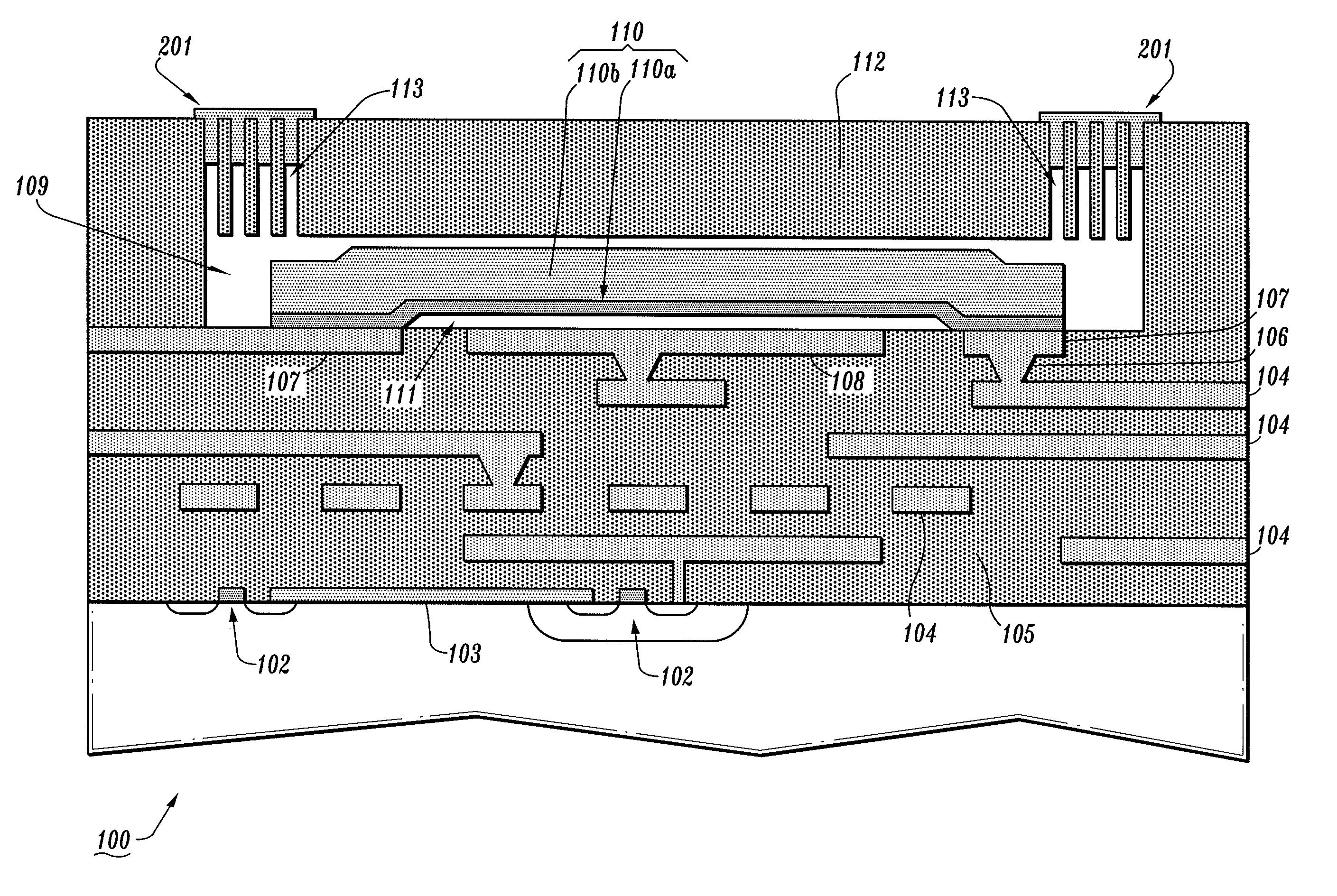
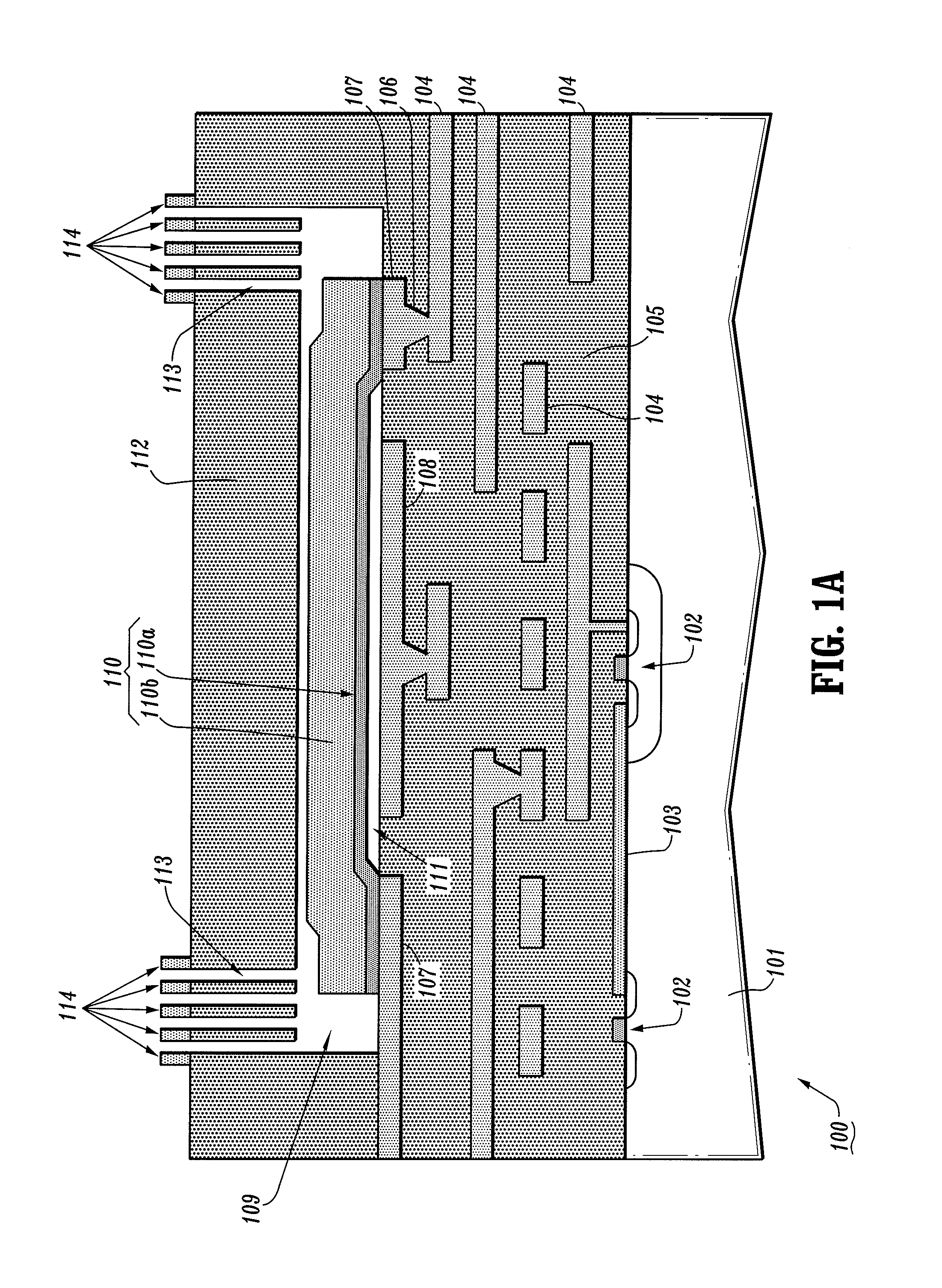
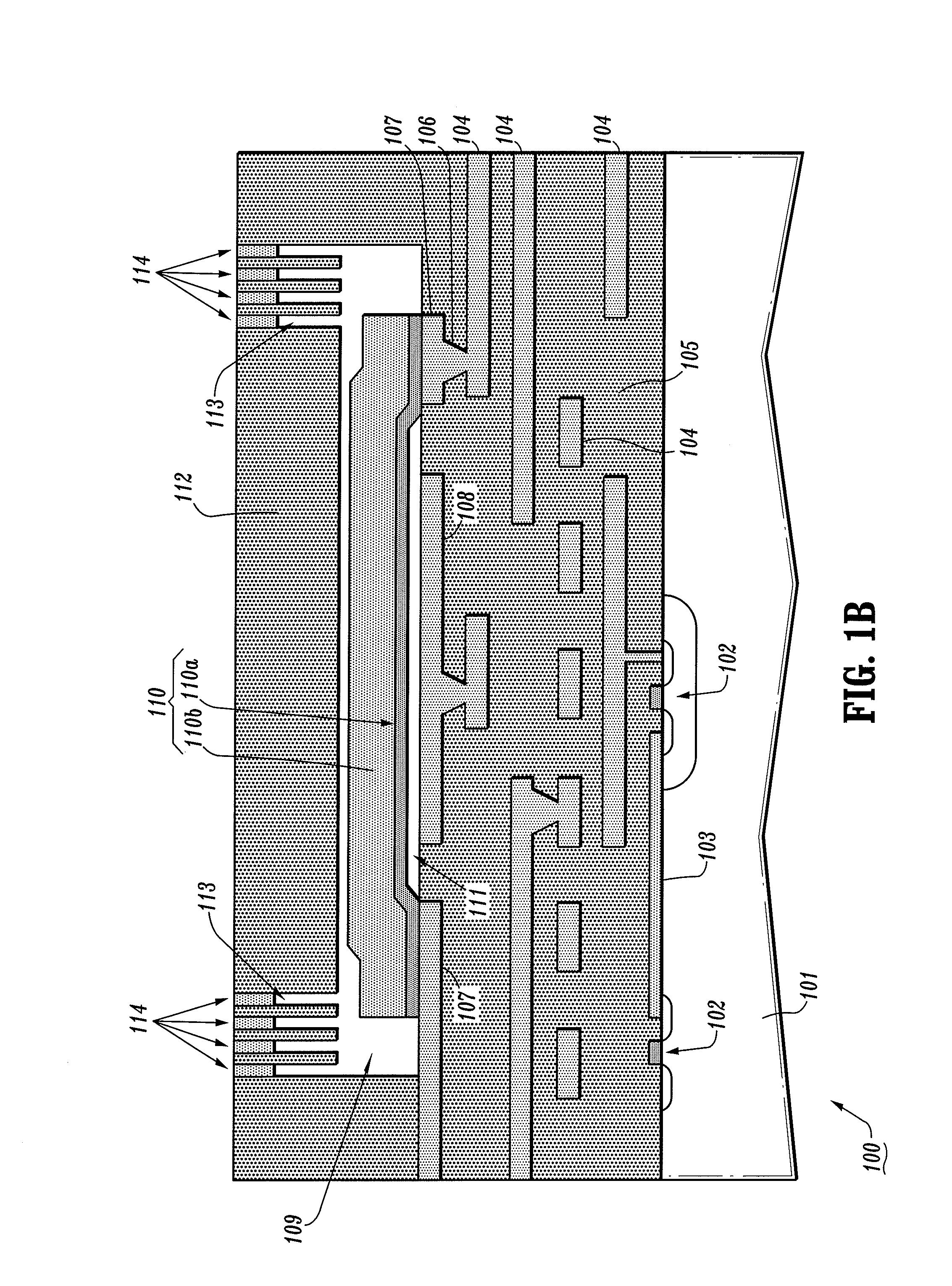
[0018]FIGS. 1A and 1B are schematic cross-sectional views of a semiconductor device (100) (e.g., device wafer) comprising monolithically integrated MEM devices and integrated circuit devices. More specifically, FIGS. 1A and 1B illustrate a method for providing wafer-scale encapsulation of MEM devices according to an exemplary embodiment of the invention. As explained below, FIGS. 1A and 1B illustrate a method for sealing fine via holes (or release holes), which are used for plasma (or other vapor phase) etching to release the MEM device and to provide a local surface micromachined cavity for hermetically sealing the MEM device in a cavity containing a desired ambient. As will be explained in detail hereafter, the exemplary method comprises depositing a reflowable material around the fine via holes which are used to release an MEM device, and then reflowing the deposited material in a vacuum, or a controlled ambient, to seal the holes.

[0019]More specifically, referring to FIG. 1A, an...


PUM


Abstract

Apparatus and methods are provided for enabling wafer-scale encapsulation of microelectromechanical (MEM) devices (e.g., resonators, filters) to protect the MEMs from the ambient and to provide either a controlled ambient or a reduced pressure. In particular, methods for wafer-scale encapsulation of MEM devices are provided, which enable encapsulation of MEM devices under desired ambient conditions that are not determined by the deposition conditions of a sealing process in which MEM release via holes are sealed or pinched-off, and which prevent sealing material from being inadvertently deposited on the MEM device during the sealing process.

Description

TECHNICAL FIELD OF THE INVENTION[0001]The present invention relates generally to apparatus and methods for providing wafer-scale encapsulation of microelectromechanical (MEM) devices (e.g., resonators, filters) to protect the MEMs from the ambient and to provide either a controlled ambient or a reduced pressure. More specifically, the invention relates to methods for wafer-scale encapsulation of MEM devices, which enable wafer-scale encapsulation of MEM devices under desired ambient conditions that are not determined by the deposition conditions of a sealing process in which MEM release via holes are sealed or pinched-off, and which prevent sealing material from being inadvertently deposited on the MEM device during the sealing process.BACKGROUND[0002]Microelectromechanical system (MEMS) devices have the potential for great impact on the communications industry. MEMS RF switches, oscillators (resonators), filters, varactors, and inductors are a few of the devices that could replace ...

Claims


Application Information

Patent Timeline
Patent Type & Authority Patents(United States)
IPC IPC(8): H01L21/00
CPCB81C1/00293B81C2203/0145
Inventor COLGAN, EVAN G.FURMAN, BRUCE K.JAHNES, CHRISTOPHER V.
Owner IBM CORP
Why Eureka
Try Eureka