
Flip-flop circuit

a flip-flop circuit and circuit technology, applied in pulse generators, pulse techniques, instruments, etc., can solve the problems of long hold time and increase delay time of flip-flop circuits, and achieve the effect of shortening hold time and speed

Inactive Publication Date: 2008-03-18
PANASONIC CORP
View PDF9 Cites 23 Cited by
  • Summary
  • Abstract
  • Description
  • Claims
  • Application Information

AI Technical Summary

Benefits of technology

"The present invention provides a scan flip-flop circuit with a reduced number of transistors needed, which increases the operating speed. This is achieved by improving the signal input-output relationship and reducing the number of transistors in the input section. The circuit includes an input section with a plurality of transistors for receiving first logic information and outputting second logic information based on the first logic information and a control signal. The output section includes a first transistor and a second transistor connected in series, and the input selection signal is input to a third transistor. The circuit also includes a latch circuit for latching the output of the input section and a control section for producing the control signal. The technical effect of the invention is to reduce the number of transistors needed and increase the operating speed of the scan flip-flop circuit."

Problems solved by technology

However, in the scan flip-flop circuit shown in FIG. 8, a maximum of four N-type transistors are connected together in series, thereby increasing the delay time.
Thus, the flip-flop circuits have a long hold time.

Method used


Image

  • Flip-flop circuit
  • Flip-flop circuit
  • Flip-flop circuit

Examples


embodiment 1

[0045]A flip-flop circuit according to Embodiment 1 of the present invention will now be described with reference to the drawings.

[0046]While the present invention will be described below primarily with respect to applications where the present invention is used as a scan flip-flop circuit, the present invention may be used as an ordinary flip-flop circuit with a 2-input selector.

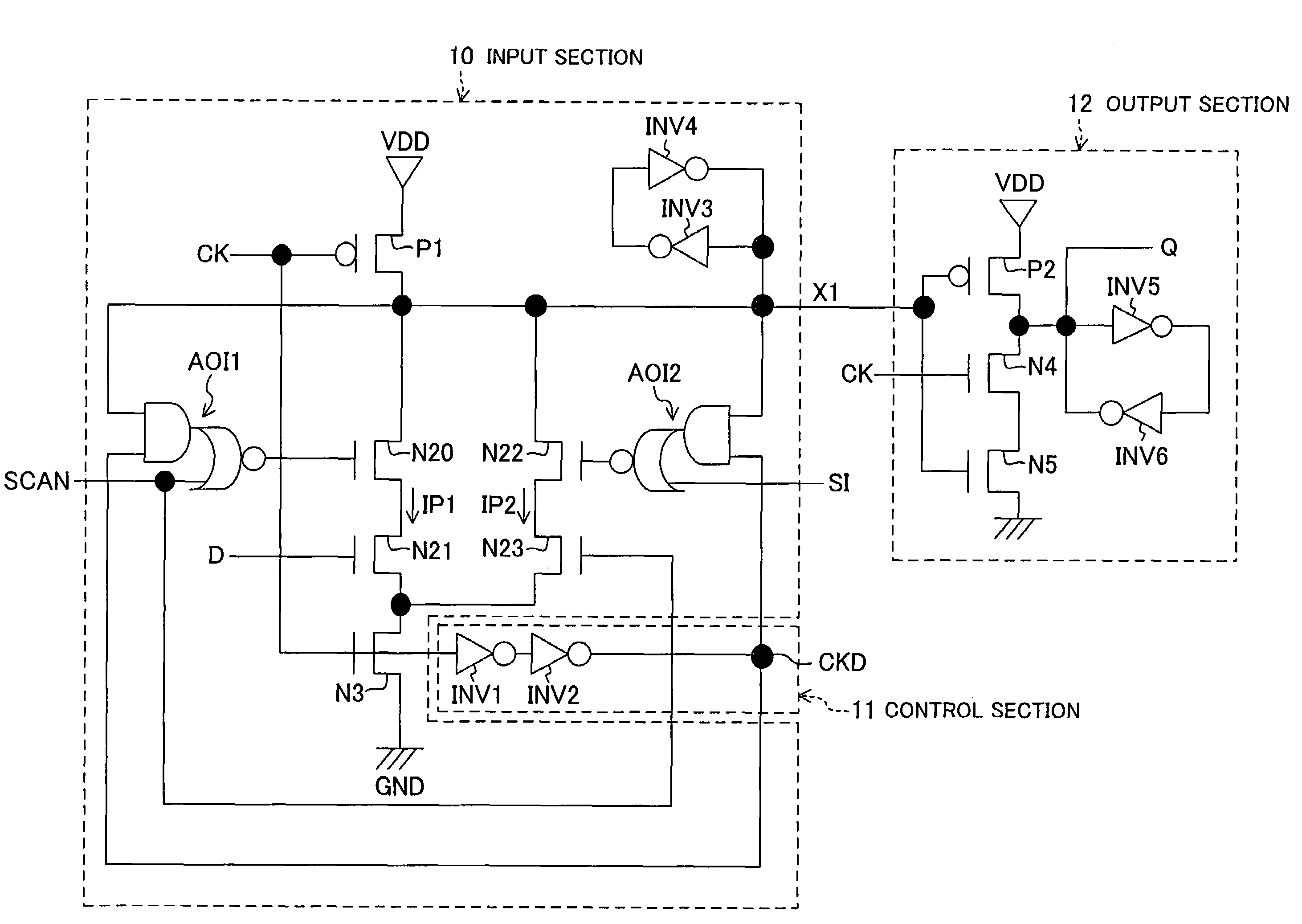
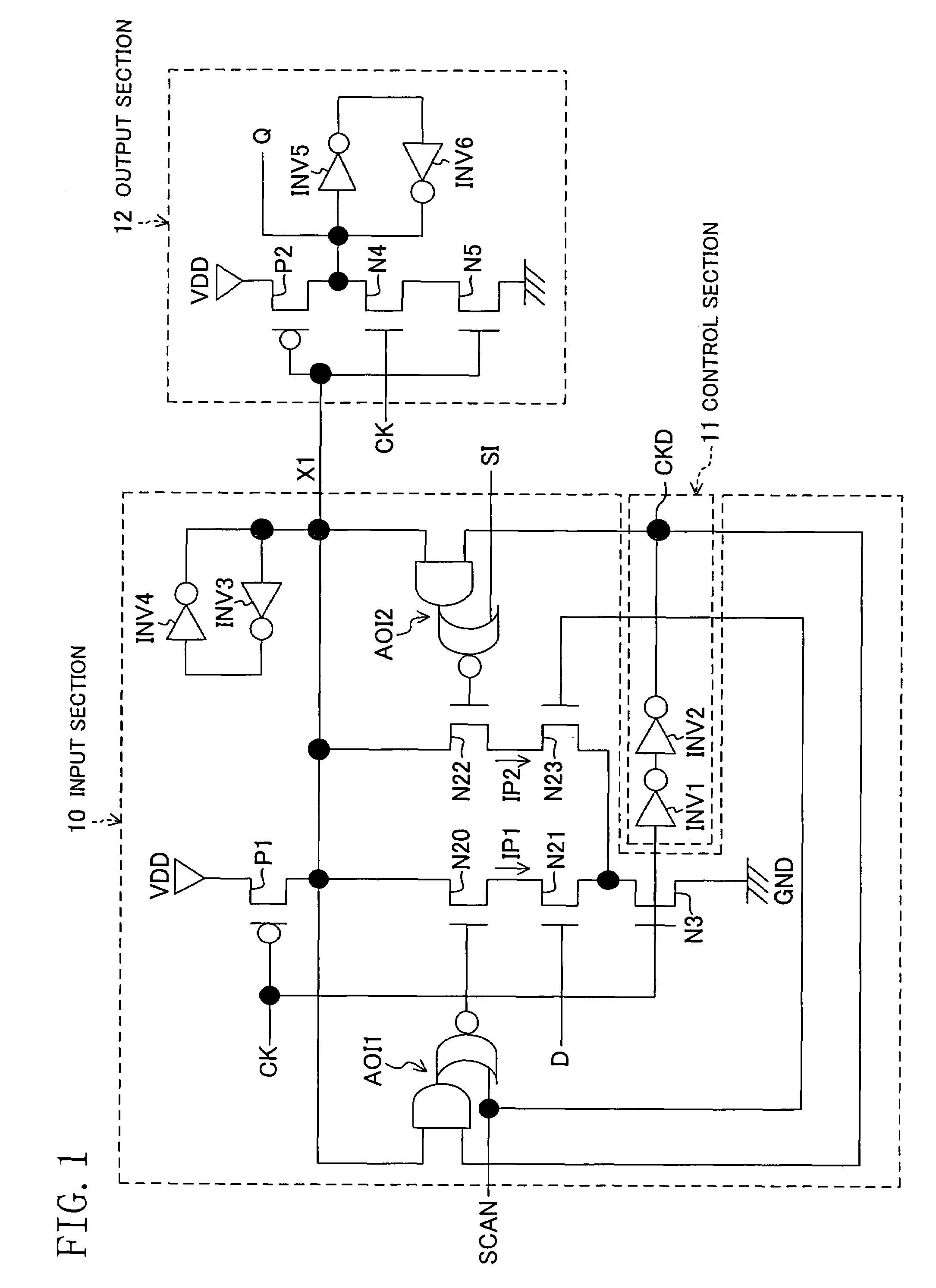
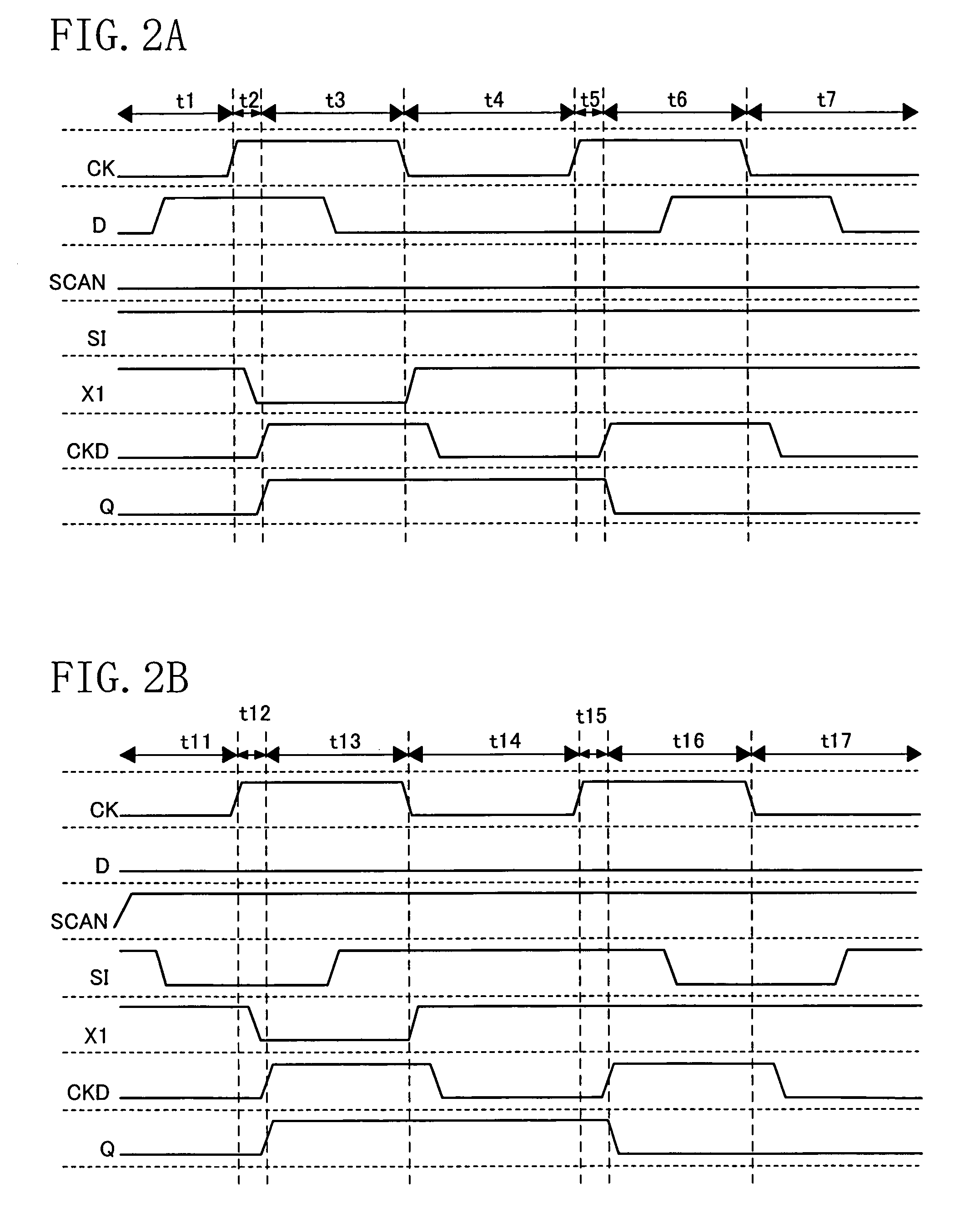
[0047]FIG. 1 is a circuit diagram showing a scan flip-flop circuit of the present embodiment, and FIGS. 2A and 2B are timing diagrams showing the operation thereof.

[0048]In FIG. 1, D denotes a data signal (the first data signal), CK a clock signal, SI a test input signal (the second data signal), SCAN a test selection signal (the input selection signal), Q an output signal, CKD a node, X1 a node, VDD the power supply, and GND the ground.

[0049]In FIG. 1, 10 denotes an input section using a dynamic circuit, 11 a control section, and 12 an output section using a static circuit. The scan flip-flop circuit inclu...

embodiment 2

[0070]A scan flip-flop circuit according to Embodiment 2 of the present invention will now be described with reference to the drawings.

[0071]FIG. 4 is a circuit diagram showing a scan flip-flop circuit of the present embodiment, and FIGS. 5A and 5B are timing diagrams showing the operation thereof.

[0072]In FIG. 4, D denotes a data signal (the first data signal), CK a clock signal, SI a test input signal (the second data signal), SCAN a test selection signal (the input selection signal), Q an output signal, NQ an inverted output signal, X1 to X4 nodes, VDD the power supply (the first potential supply node) of a predetermined power supply potential (the first potential), and GND the ground (the second potential supply node).

[0073]In FIG. 4, 20 denotes an input section, 21 a latch circuit, 22 a control section having a node (the first node) X2, and 23 an output section. The scan flip-flop circuit includes P-type transistors (the transistors of the first polarity) P1 to P5, N-type trans...

embodiment 3

[0093]A scan flip-flop circuit according to Embodiment 3 of the present invention will now be described with reference to the drawings.

[0094]FIG. 6 is a circuit diagram showing a scan flip-flop circuit of the present embodiment. In the configuration of FIG. 6, one or more of the P-type transistors are shared between the NOR circuits NR1 and NR2 of the flip-flop circuit, as compared with that of Embodiment 2 shown in FIG. 4. In the present embodiment, like elements to those of Embodiment 2 will be denoted by like reference numerals and will not be further described below. In FIG. 6, P6 to P8 denote P-type transistors, and N9 to N12 N-type transistors. The P-type transistor P6 is the transistor that is shared between the NOR circuits NR1 and NR2.

[0095]While the NOR circuits NR1 and NR2 shown in FIG. 4 require eight transistors, the present embodiment realizes a similar function with seven transistors, including the P-type transistors P6 to P8 and the N-type transistors N9 to N12.

[0096...


PUM


Abstract

A scan flip-flop circuit including an input section employing a dynamic circuit and an output section employing a static circuit, capable of latching in data within a period of a pulse width that is shorter than the clock cycle, wherein only three N-type transistors are connected in series in the input section employing a dynamic circuit. A data signal is input directly to one of the three N-type transistors. On the other hand, a test input signal is input to an AND / OR inverter circuit. The AND / OR inverter circuit receives, as a control signal, the potential of the node obtained as the clock signal passes through two inverter circuits. Therefore, there is required only a short hold time for the test input signal.

Description

CROSS REFERENCE TO RELATED APPLICATION[0001]This Non-provisional application claims priority under 35 U.S.C. §119(a) on Patent Application No. 2005-211690 filed in Japan on Jul. 21, 2005, the entire contents of which are hereby incorporated by reference.BACKGROUND OF THE INVENTION[0002]The present invention relates to a flip-flop circuit that operates at a high speed and can be configured with a small number of transistors. More particularly, the present invention relates to a flip-flop circuit capable of selectively storing one of a plurality of data inputs or a flip-flop circuit with a scan function.[0003]Flip-flop circuits account for a significant part, among other logic circuits in a semiconductor integrated circuit, in terms of the area, the power consumption and the critical path delay. Accordingly, there is a demand for a flip-flop circuit with a smaller area, a lower power consumption and a higher speed. Particularly, scan flip-flop circuits are often used for easy testing ...

Claims


Application Information

Patent Timeline
Patent Type & Authority Patents(United States)
IPC IPC(8): H03K3/356
CPCG01R31/318541H03K3/012H03K3/0375H03K3/356139
Inventor HIRATA, AKIO
Owner PANASONIC CORP
Learn More