Semiconductor device

a technology of semiconductor devices and dielectric devices, applied in the direction of information storage, static storage, digital storage, etc., can solve the problems of increasing operating power, wasteful current flowing through the bitline pair, and difficult optimization of timing design, so as to reduce wasteful power consumption

Active Publication Date: 2008-03-18
RENESAS ELECTRONICS CORP
View PDF6 Cites 21 Cited by
  • Summary
  • Abstract
  • Description
  • Claims
  • Application Information

AI Technical Summary

Benefits of technology

[0011]It is an object of the present invention to provide a semiconductor device capable of reducing wasteful power consumption.
[0013]The semiconductor device according to the foregoing aspect of the invention has an advantage of reducing unnecessary power consumption because it is provided with the mitigating means for mitigating the potential change or the current change in the first signal lines during the period in which the sense amplifier circuit is being activated.
[0014]The present invention provides, in accordance with another aspect, a semiconductor device including a plurality of memory units that do not require a refresh operation, and a central processing unit. Each of the memory units includes: memory circuits for storing data, arranged in a matrix form; first signal lines for reading the data from the memory circuits; second signal lines for transferring a signal that controls connection between the memory circuits and the first signal lines; a sense amplifier circuit for reading and determining data by detecting a potential change or a current change in the first signal lines; and mitigating means for mitigating the potential change or the current change in the first signal lines during a period in which the sense amplifier circuit is being activated. The central processing unit controls the memory units. The mitigating means mitigates the potential change or the current change in the first signal lines even when a memory unit selecting signal supplied from the central processing unit to the memory units is in an unselected state.
[0015]The semiconductor device according to the foregoing aspect of the invention has an advantage of reducing unnecessary power consumption further because it mitigates the potential change or the current change in the first signal lines even when the memory units are in a standby state.

Problems solved by technology

With this tendency, the increase in operating power has been a problem in the SRAMs and the like.
However, in order to deactivate the wordline with that timing, optimization in timing design is difficult; thus, it has been necessary to provide an operation margin when taking process variations and the like into consideration.
This causes a problem that a wasteful current flows through the bitline pair and a more power than is necessary is required in precharging.
The method proposed in the foregoing reference, however, merely intends to locally control the time for deactivating a wordline using the replica bitline, and it does not necessarily guarantee that the time for determining data is always earlier than the time for deactivating the wordline.
If the time for determining data becomes later, a sufficient potential difference in a bitline pair cannot be obtained and consequently correct data may not be read out by the sense amplifier circuit.
That is, even with the method proposed in the foregoing reference, the potential of the bitline pair continues to reduce during the time from the time data is determined until the wordline is deactivated because an operation margin needs to be ensured, and consequently unnecessary power is wasted.

Method used


Image

  • Semiconductor device
  • Semiconductor device
  • Semiconductor device

Examples


first preferred embodiment

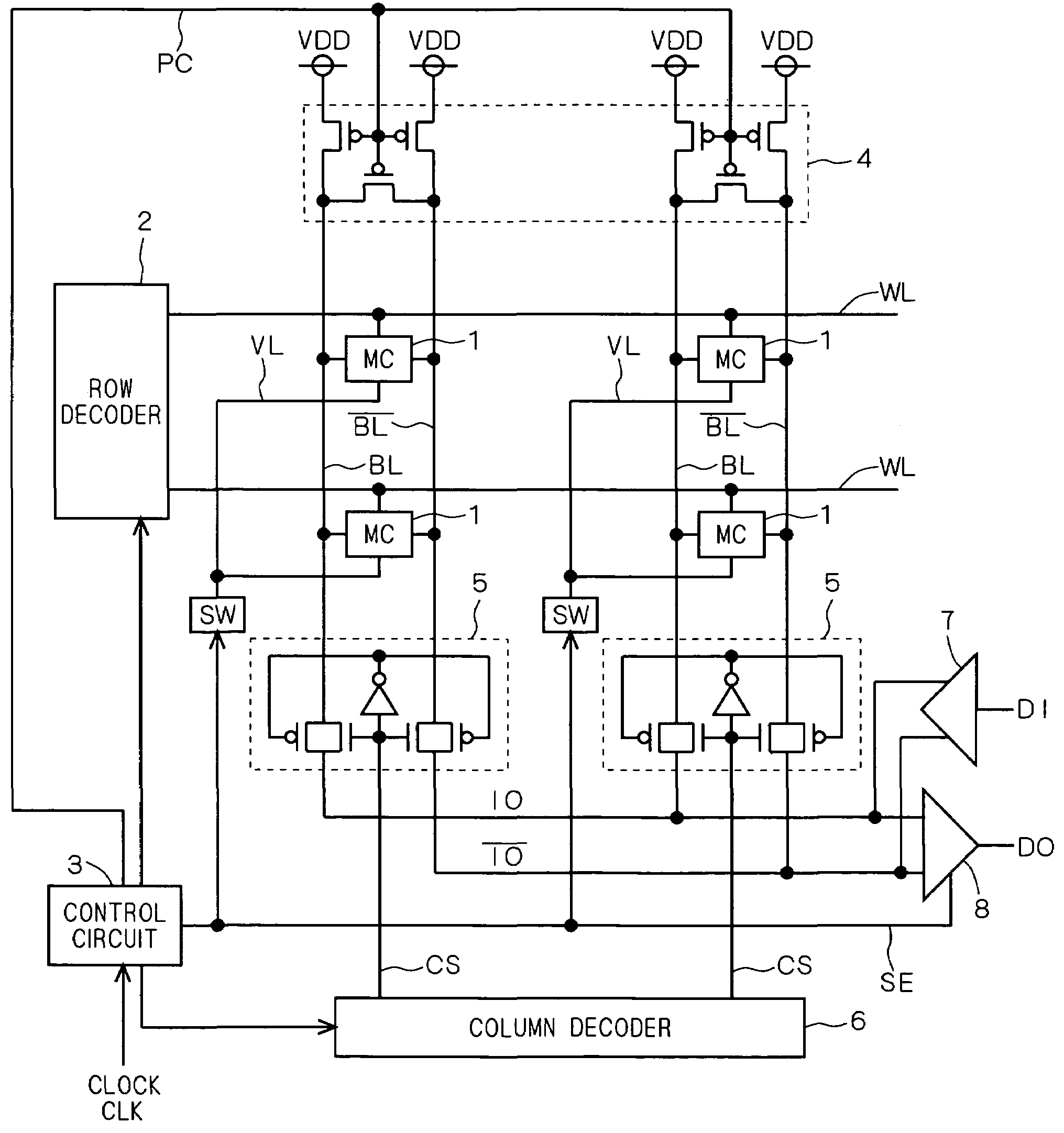
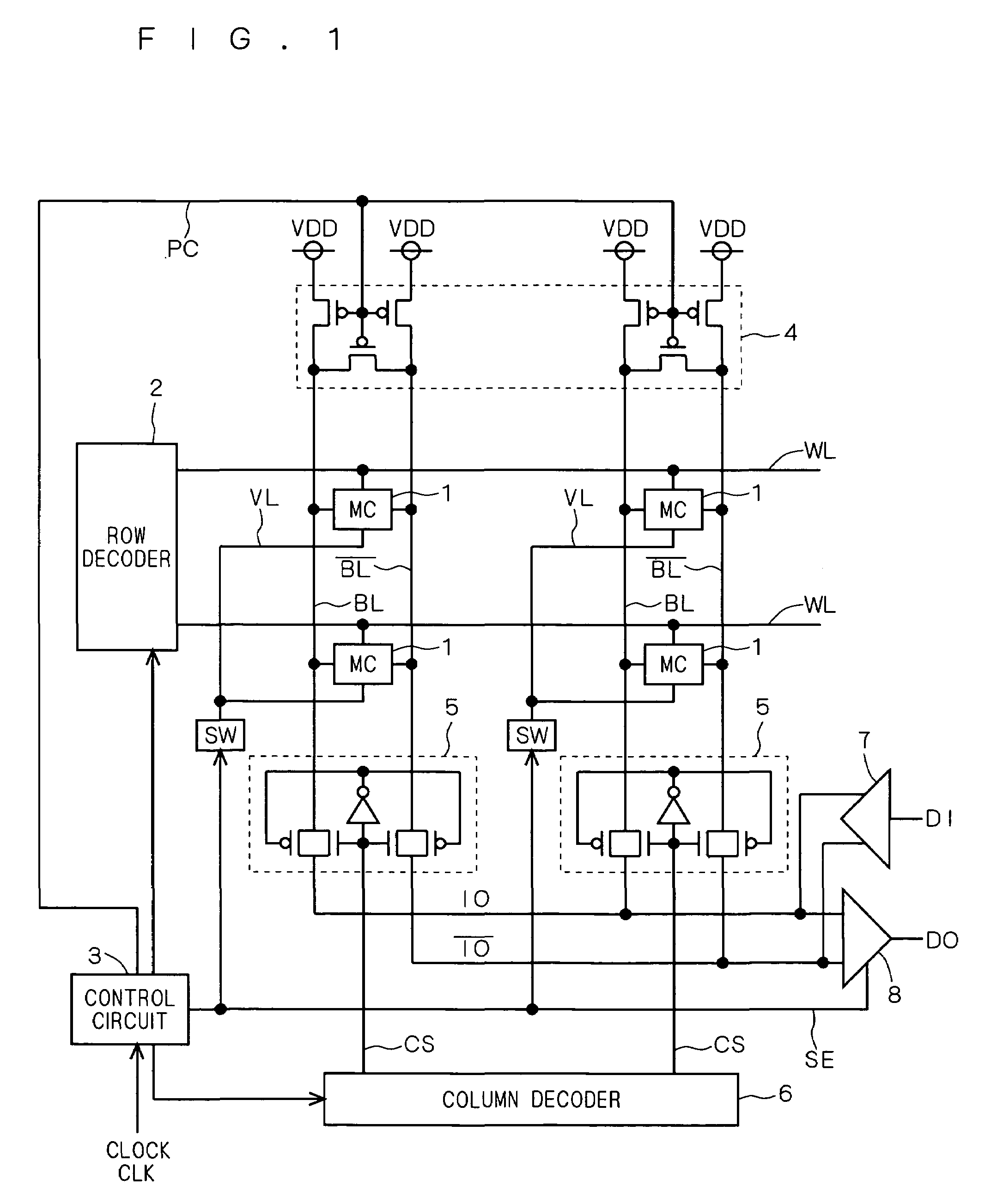
[0053]The semiconductor device according to the present preferred embodiment is a semiconductor device having a memory unit. FIG. 1 illustrates a configuration diagram of a memory unit of the semiconductor device according to the present preferred embodiment (hereinafter also simply referred to as a “semiconductor device”). In the present preferred embodiment, the description assumes that the memory unit is a SRAM. It should be noted, however, that the present invention is not limited to SRAMs but may be applied to other memories such as multi-port memories and ROMs (Read Only Memories) as long as the memory units do not require refresh operations.

[0054]Referring to FIG. 1, the memory unit includes memory cells 1 arranged in a matrix form, and each of the memory cells 1 is connected to wordlines WL and a bitline pair BL and BL. In the semiconductor device shown in FIG. 1, the wordlines WL are connected to a row decoder 2, and the row decoder 2 is connected to a control circuit 3. On...

second preferred embodiment

[0082]Next, a second preferred embodiment is described. In the first preferred embodiment, the memory cell potential controlling circuits SW carry out the same operation for all the columns irrespective of whether or not the column is selected by the column decoder 6. In the present preferred embodiment, the memory cell potential controlling circuits SW perform different control operations for memory cells 1 that are to be read out and for memory cells 1 that are not read out.

[0083]FIG. 8 shows a configuration diagram of a semiconductor device according to the present preferred embodiment. The configuration diagram shown in FIG. 8 is basically the same as that shown in FIG. 1, and the present preferred embodiment also describes an SRAM as an example.

[0084]First, the semiconductor device shown in FIG. 8 includes memory cells 1 arranged in a matrix form, and each of the memory cells 1 is connected to a wordline WL and a bitline pair BL and BL. In the semiconductor device shown in FIG....

third preferred embodiment

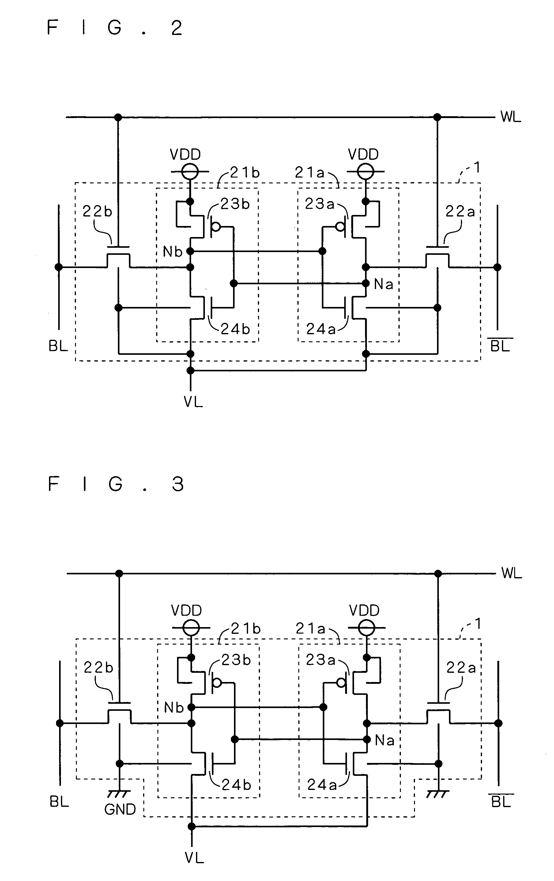
[0098]Next, a third preferred embodiment is described. A semiconductor device according to the present preferred embodiment has a configuration in which the circuit of the memory cell 1 shown in FIG. 2 or 3, discussed in the first preferred embodiment, is replaced with a circuit of a memory cell 1 shown in FIG. 11 or 12. The memory cell 1 shown in FIG. 11 includes inverters 21a and 21b that constitute an inverter latch for storing data, and NMOSs 22a and 22b the gates of which are connected to a wordline WL. The NMOS 22a connects a bitline BL with the inverter 21a, while the NMOS 22b connects a bitline BL with the inverter 21b.

[0099]The inverter 21a includes a PMOS 23a connected between a VL line and a node Na, and an NMOS 24a connected between the node Na and GND. The inverter 21b includes a PMOS 23b connected between the VL line and a node Nb, and an NMOS 24b connected between the node Nb and GND.

[0100]Both the gates of the PMOS 23a and the NMOS 24a are connected to the node Nb, ...


PUM


Abstract

The invention provides a semiconductor device capable of reducing wasteful power consumption. The semiconductor device of the invention does not require a refresh operation, and includes memory circuits for storing data, arranged in a matrix form, first signal lines for reading data from the memory circuits, second signal lines for transferring a signal that controls connection between the memory circuits and the first signal lines, a sense amplifier circuit for reading and determining data by detecting a potential change or a current change in the first signal lines, and a mitigating means for mitigating the potential change or the current change in the first signal lines during a period in which the sense amplifier circuit is being activated.

Description

BACKGROUND OF THE INVENTION[0001]1. Field of the Invention[0002]The present invention relates to semiconductor devices, and more particularly to a semiconductor device having a memory unit that is capable of reducing power consumption.[0003]2. Description of the Background Art[0004]In recent years, static random access memories (hereinafter also referred to as SRAMs), multi-port memories, and the like that are incorporated in system LSIs or the like tend to have a larger storage scale and a higher operating frequency. With this tendency, the increase in operating power has been a problem in the SRAMs and the like. With the SRAMs and the like, the charge / discharge current caused by the oscillation of a signal in bitlines takes up a large proportion in the operating power. Thus, in order to reduce the operating power in SRAMs and the like, it is important to reduce the charge / discharge current in the bitlines.[0005]In the case of SRAM, as the potential of a wordline rises in reading d...

Claims


Application Information

Patent Timeline
Patent Type & Authority Patents(United States)
IPC IPC(8): G11C11/00
CPCG11C11/412G11C11/413
Inventor TSUKAMOTO, YASUMASANII, KOJI
Owner RENESAS ELECTRONICS CORP
Why Eureka
Try Eureka