Semiconductor device and method for fabricating the same

a technology of semiconductors and semiconductors, applied in the direction of semiconductor devices, basic electric elements, electrical equipment, etc., can solve the problems of low operation power of electronic equipment, inability to perfectly control the short channel effect with the ldd structure, and inability to achieve the effect of preventing the short channel

Active Publication Date: 2008-03-25
MARVELL ASIA PTE LTD +1
View PDF2 Cites 35 Cited by
  • Summary
  • Abstract
  • Description
  • Claims
  • Application Information

AI Technical Summary

Benefits of technology

[0013]An object of the present invention is to provide a minute transistor and a method for fabricat...

Problems solved by technology

According to the decrease of the channel length in the semiconductor device, there may be the undesirable electric characteristics, for example, a short channel effect.
However, on the decrease in size of the semiconductor device, an operation power for electronic equipment is not low.
For example, in case of an NMOS transistor, injected electrons of the source are excessively accelerated in state of a high potential gradient, so that hot carriers...

Method used


Image

  • Semiconductor device and method for fabricating the same
  • Semiconductor device and method for fabricating the same
  • Semiconductor device and method for fabricating the same

Examples


first embodiment

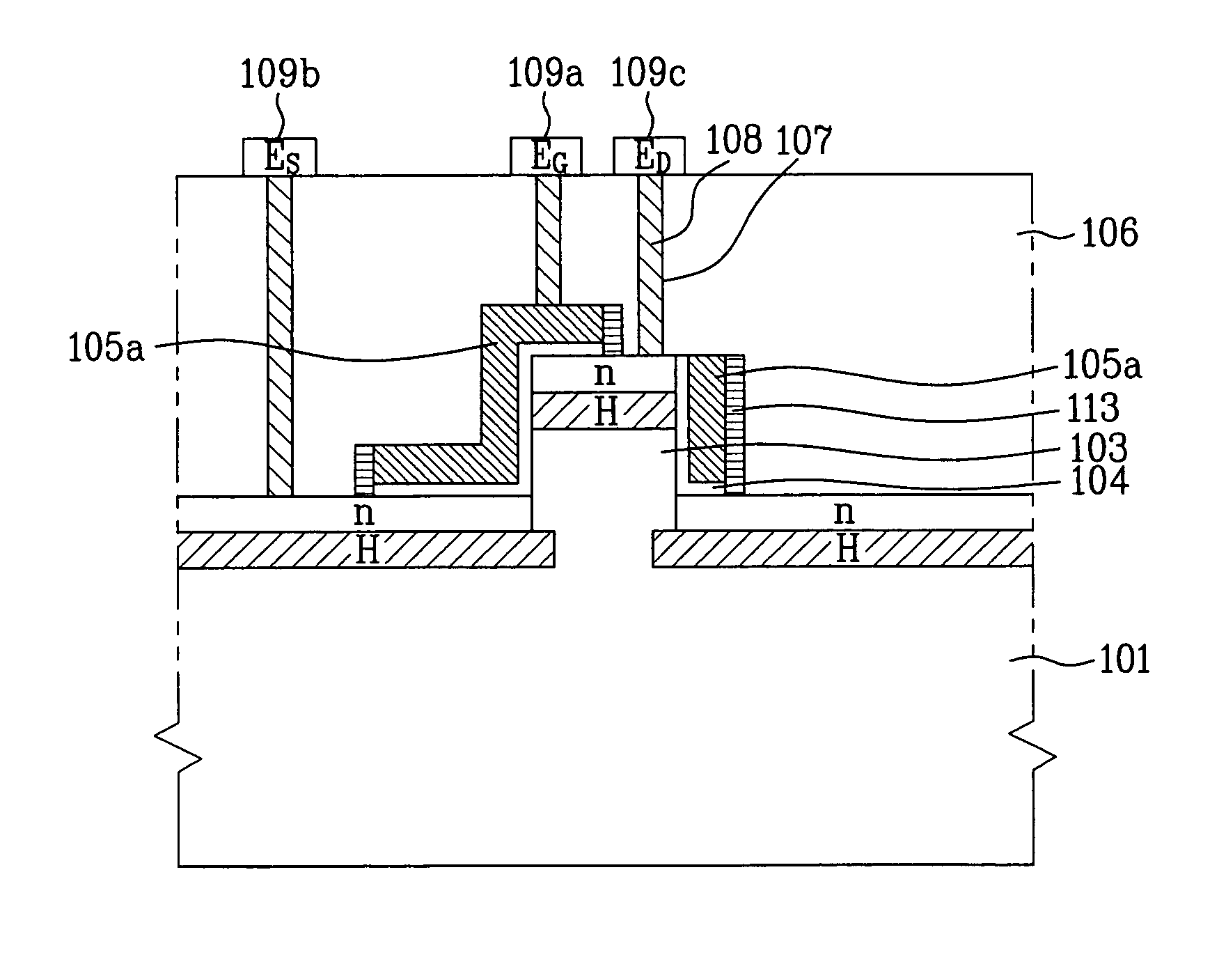
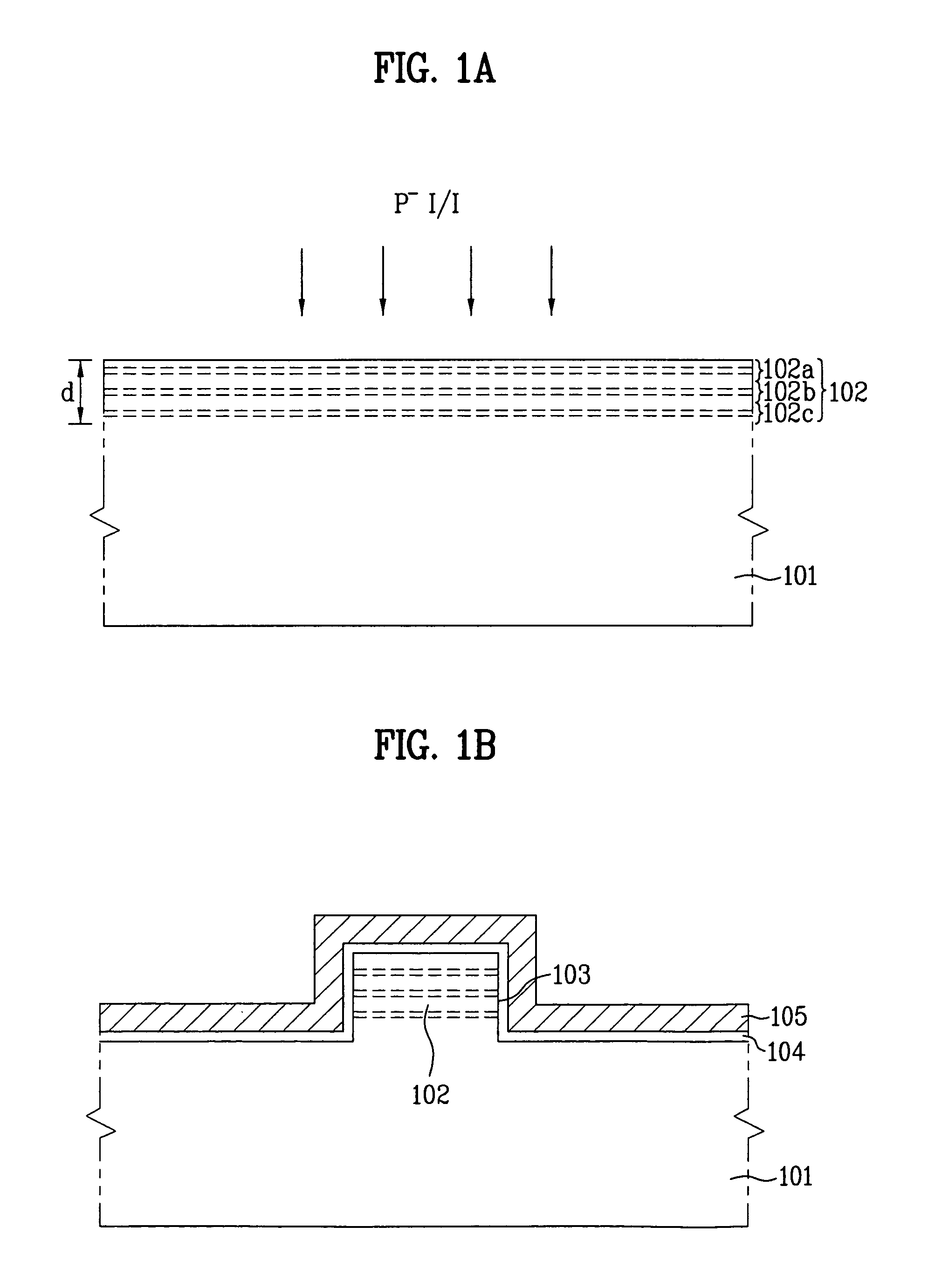
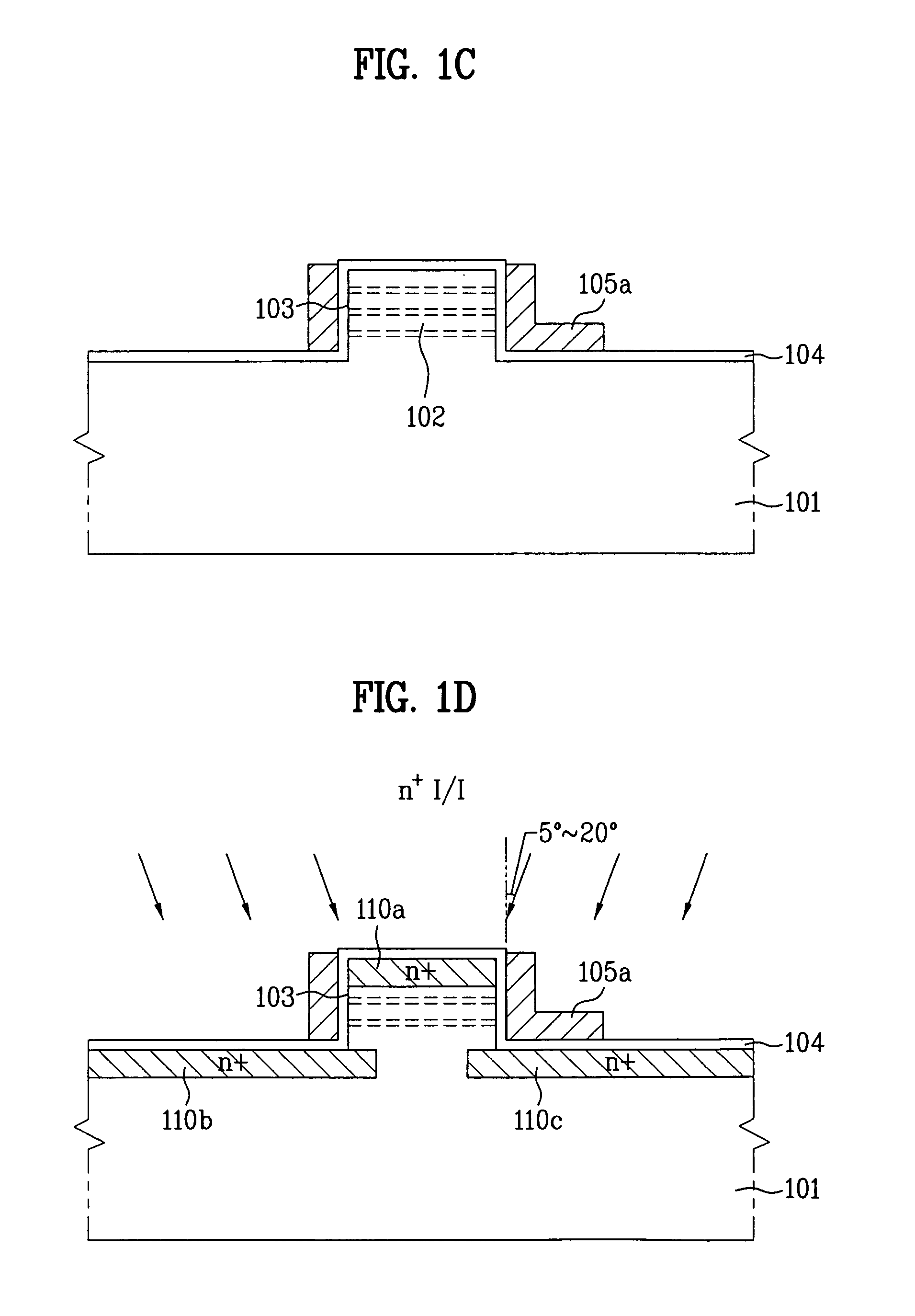
[0039]FIG. 1A to FIG. 1E show cross sectional views of the fabrication process for a vertical transistor according to the present invention.

[0040]First, as shown in FIG. 1A, a semiconductor substrate 101 of mono-crystal silicon is prepared. The semiconductor substrate 101 may be n-type or p-type mono-crystal silicon substrate. For convenience of explanation, herein, the p-type mono-crystal silicon substrate will be described as follows.

[0041]In this case, channel ion implantation process is performed to the semiconductor substrate 101 third times, so as to uniformly provide channel ions in a channel ion area 102. That is, the channel ion area formed by implanting the channel ions three times corresponds to a channel of a vertical transistor.

[0042]Meanwhile, the channel ion implantation process will be described in detail.

[0043]First, first conductive (p-type) impurity ions, for example, boron B ions are implanted in a first channel ion implantation at an energy between 10 KeV and 30...

second embodiment

[0052]FIG. 2A to FIG. 2E show cross sectional views of the fabrication process for a vertical transistor according to the present invention.

[0053]In the vertical transistor according to the second embodiment of the present invention, as shown in FIG. 2A, a semiconductor substrate 101 of mono-crystal silicon is prepared. The semiconductor substrate 101 may be formed of a first conductive type mono-crystal silicon, wherein the first conductive type may be n-type or p-type. For convenience of explanation, herein, the first conductive type will be explained as the p-type.

[0054]Then, the semiconductor substrate 101 is selectively removed by dry etching such as RIE (Reactive Ion Etching) using photolithography, thereby forming a predetermined pillar 103. At this time, the semiconductor substrate 101 is etched at a thickness between about 1 μm and 2 μm. Also, although not shown, a buffering oxide layer may be deposited on an entire surface of the semiconductor substrate 101 before the dry ...

third embodiment

[0062]FIG. 3A to FIG. 3C show cross sectional views of the fabrication process for a vertical transistor according to the present invention.

[0063]As shown in FIG. 3A, a sacrificial oxide layer 202 is formed on an entire surface of a p-type mono-crystal silicon semiconductor substrate 201 by spin coating or low-pressure CVD, wherein the sacrificial oxide layer 202 is formed at a thickness between 1000 Å and 5000 Å. Then, a photoresist layer is coated on the sacrificial oxide layer 202, and an exposure and development process is performed thereto, thereby forming a photoresist pattern 203 for exposing a predetermined portion of the sacrificial oxide layer 202. After that, the sacrificial oxide layer 202 is selectively removed to expose the semiconductor substrate 201 by using the photoresist pattern 203 as an etching mask, thereby forming an aperture 202a.

[0064]As shown in FIG. 3B, after removing the photoresist pattern 203, a polysilicon layer 204 is formed in the aperture 202a at a...


PUM


Abstract

A transistor and a method for fabricating the same is disclosed, to uniformly provide impurity ions in impurity areas, and to prevent a short channel effect, in which the method for fabricating the transistor includes steps of forming a plurality of channel ion implantation areas having different depths in a first conductive type semiconductor substrate; forming a pillar by selectively etching the first conductive type semiconductor substrate; sequentially depositing a gate insulating layer and a conductive layer for a gate electrode on the first conductive type semiconductor substrate including the pillar; forming the gate electrode by selectively patterning the conductive layer; and forming second conductive type source/drain impurity ion areas in the first conductive type semiconductor substrate corresponding to the top of the pillar and both sidewalls of the pillar.

Description

CROSS-REFERENCE TO RELATED APPLICATIONS[0001]This application claims the benefit of Korean Application Nos. P2003-98092 and P2003-98079, filed on Dec. 27, 2003, which is hereby incorporated by reference as if fully set forth herein.BACKGROUND OF THE INVENTION[0002]1. Field of the Invention[0003]The present invention relates to a semiconductor device, and more particularly, to a vertical transistor and a method for fabricating the same, to improve operation reliability of the transistor and to realize minuteness in the semiconductor device.[0004]2. Discussion of the Related Art[0005]With high integration of a semiconductor device, a size of the semiconductor device decreases, whereby a channel length of the semiconductor device also decreases. According to the decrease of the channel length in the semiconductor device, there may be the undesirable electric characteristics, for example, a short channel effect.[0006]In order to overcome the short channel effect, it is necessary to real...

Claims


Application Information

Patent Timeline
IPC IPC(8): H01L21/336H01L21/20H01L21/265H01L29/78
CPCH01L21/26586H01L29/66666H01L29/7827H01L21/2022
Inventor KIM, HAG DONG
Owner MARVELL ASIA PTE LTD
Why Eureka
Try Eureka