Composite field effect transistor

a field effect transistor and composite material technology, applied in the field of composite field effect transistors, can solve the problems of undesirable high current flow in most applications, jfets in depletion mode require a negative gate-to-source potential to turn off, and mosfets are generally not the most cost-efficient devices

Inactive Publication Date: 2008-03-25
POWER INTEGRATIONS INC
View PDF4 Cites 55 Cited by
  • Summary
  • Abstract
  • Description
  • Claims
  • Application Information

AI Technical Summary

Benefits of technology

[0005]Embodiments of the present invention provide a composite field effect transistor that includes a zener diode, a junction field effect transistor and a metal-oxide-semiconductor field effect transistor. A gate of the junction field effect transistor is coupled to an anode of the zener diode. A cathode of the zener diode is coupled to a gate of the metal-oxide-semiconductor field effect transistor. A drain of the metal-oxide-semiconductor field effect transistor is coupled to a source of the junction field effect transistor. In one implementation, the junction field effect transistor is a depletion mode device and the metal-oxide-semiconductor field effect transistor is an n-channel enhancement mode device.

Problems solved by technology

However, depletion mode JFETs require a negative gate-to-source potential to turn off.
Accordingly, when a system incorporating a JFET is first turned on, the depletion mode JFET is also on, causing undesirable high current to flow in most applications.
However, MOSFETs are generally not normally the most cost-efficient devices for high voltage (>100V) applications.

Method used


Image

  • Composite field effect transistor
  • Composite field effect transistor
  • Composite field effect transistor

Examples


Embodiment Construction

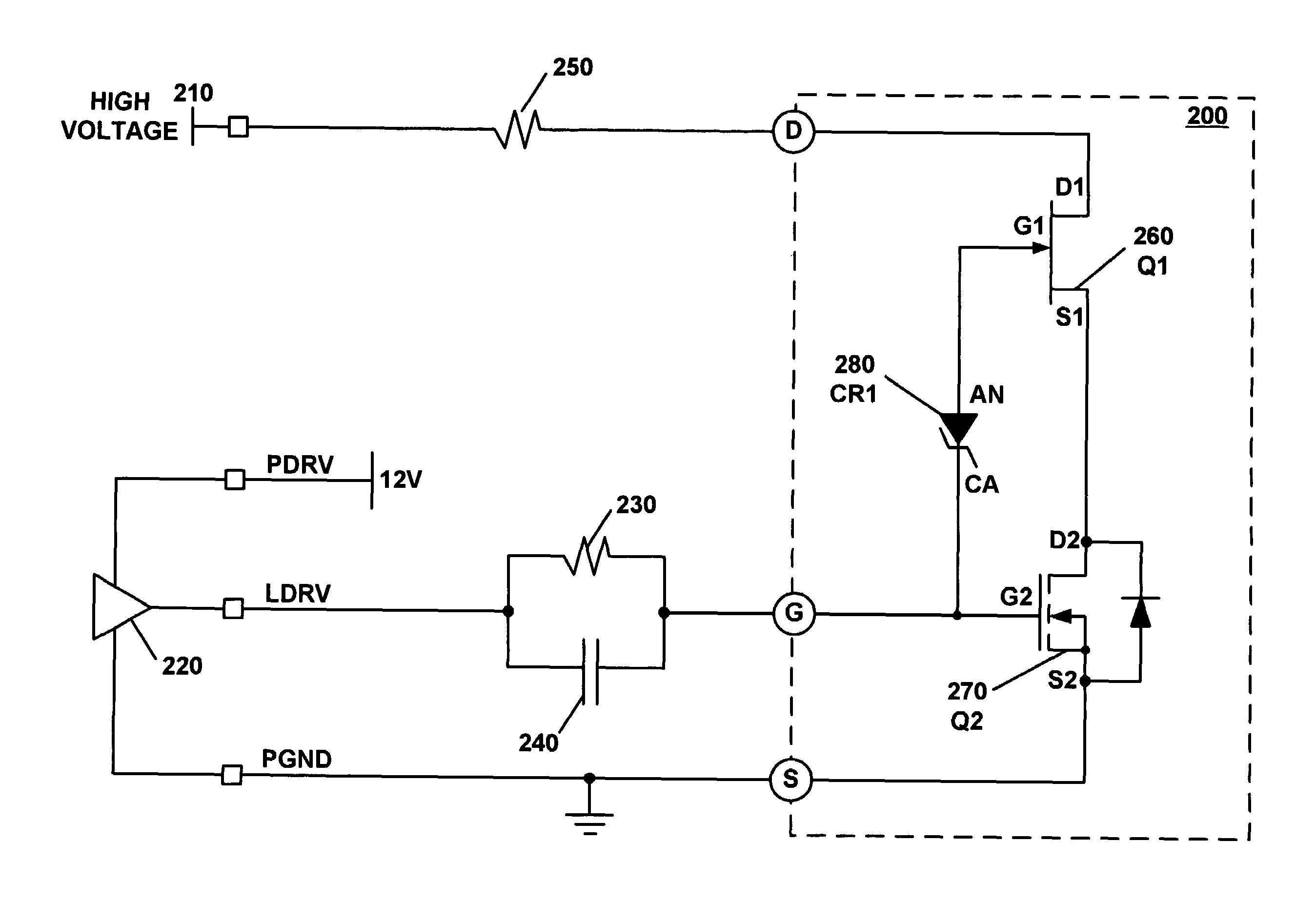
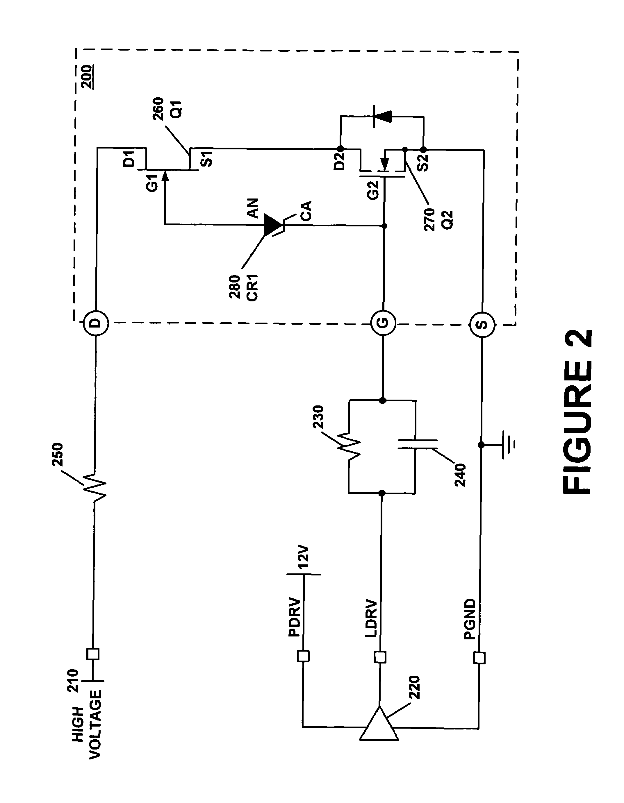
[0009]Reference will now be made in detail to the embodiments of the invention, examples of which are illustrated in the accompanying drawings. While the invention will be described in conjunction with these embodiments, it will be understood that they are not intended to limit the invention to these embodiments. On the contrary, the invention is intended to cover alternatives, modifications and equivalents, which may be included within the scope of the invention as defined by the appended claims. Furthermore, in the following detailed description of the present invention, numerous specific details are set forth in order to provide a thorough understanding of the present invention. However, it is understood that the present invention may be practiced without these specific details. In other instances, well-known methods, procedures, components, and circuits have not been described in detail as not to unnecessarily obscure aspects of the present invention.

[0010]FIG. 1 shows a diagram...


PUM


Abstract

A composite field effect transistor, in accordance with one embodiment, includes a zener diode, a junction field effect transistor and a metal-oxide-semiconductor field effect transistor. A gate of the junction field effect transistor is coupled to an anode of the zener diode. A cathode of the zener diode is coupled to a gate of the metal-oxide-semiconductor field effect transistor. A drain of the metal-oxide-semiconductor field effect transistor is coupled to a source of the junction field effect transistor.

Description

CROSS-REFERENCE TO RELATED APPLICATIONS[0001]This application claims the benefit of U.S. Provisional Application No. 60 / 663,315 filed Mar. 18, 2005.BACKGROUND OF THE INVENTION[0002]Depletion mode junction field effect transistors (JFETs) are efficient semiconductor structures, especially for high-voltage switching applications. However, depletion mode JFETs require a negative gate-to-source potential to turn off. Accordingly, when a system incorporating a JFET is first turned on, the depletion mode JFET is also on, causing undesirable high current to flow in most applications.[0003]An enhancement mode metal-oxide-semiconductor field effect transistor (MOSFET), on the other hand, requires a positive voltage to turn on. Therefore, the MOSFET, being a normally off device, does not typically exhibit high current flows in most applications upon start-up. However, MOSFETs are generally not normally the most cost-efficient devices for high voltage (>100V) applications.[0004]Accordingly,...

Claims


Application Information

Patent Timeline
Patent Type & Authority Patents(United States)
IPC IPC(8): H03K17/687
CPCH03K17/08148H03K17/107H03K17/302
Inventor KLEIN, JONATHANTSOU, MORRIS
Owner POWER INTEGRATIONS INC
Why Eureka
Try Eureka