Insulated gate type source-leakage composite field plate transistor with high electron mobility and preparing method thereof

A high electron mobility, insulating gate type technology, applied in the field of microelectronics, can solve the problems of reducing the yield of the device, complicated manufacturing process, increasing the difficulty of the device, etc., to improve the breakdown voltage, large drain-source voltage, and enhance reliability. Effect

Inactive Publication Date: 2009-04-22
XIDIAN UNIV
View PDF0 Cites 13 Cited by
  • Summary
  • Abstract
  • Description
  • Claims
  • Application Information

AI Technical Summary

Problems solved by technology

However, the manufacturing process of the high electron mobility transistor using the stacked field plate structure is relatively complicated. Each additional layer of field plate requires additional process steps such as photolithography, metal deposition, insulating dielectric material deposition, stripping, and cleaning. To make the insulating dielectric material deposited under the field plates of each layer have an appropriate thickness, cumbersome process debugging must be carried out, thus greatly increasing the difficulty of device manufacturing and reducing the yield of devices

Method used


Image

  • Insulated gate type source-leakage composite field plate transistor with high electron mobility and preparing method thereof
  • Insulated gate type source-leakage composite field plate transistor with high electron mobility and preparing method thereof
  • Insulated gate type source-leakage composite field plate transistor with high electron mobility and preparing method thereof

Examples


Embodiment 1

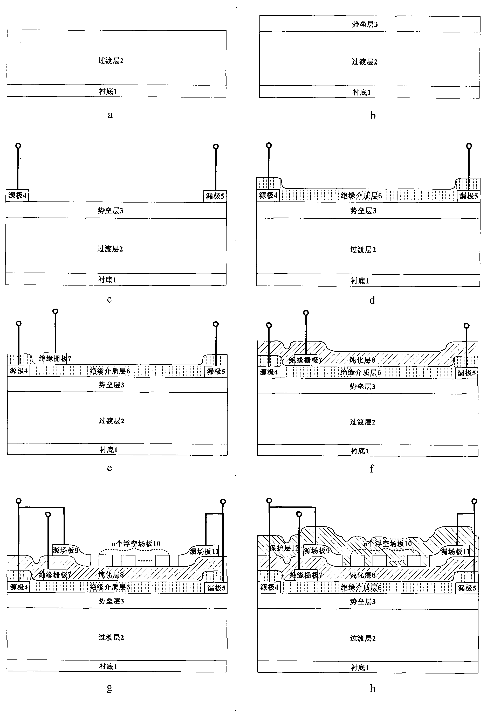
[0057] The production substrate is sapphire, and the insulating dielectric layer is SiO 2 , the passivation layer is SiN, the protective layer is SiN, the source field plate, the drain field plate and each floating field plate are Ti / Au metal composite field plate high electron mobility transistors, and the process is:

[0058] 1. Epitaxial undoped transition layer 2 with a thickness of 1 μm on sapphire substrate 1 by metal organic chemical vapor deposition technology, the transition layer is composed of GaN materials with thicknesses of 45 nm and 0.955 μm from bottom to top. The process conditions adopted for the epitaxial lower layer GaN material are: temperature 545°C, pressure 150 Torr, hydrogen gas flow rate 5400 sccm, ammonia gas flow rate 5400 sccm, gallium source flow rate 45 μmol / min; the process conditions adopted for the epitaxial upper layer GaN material are: temperature 1080°C, pressure 150 Torr, hydrogen flow rate 5400 sccm, ammonia gas flow rate 5400 sccm, galli...

Embodiment 2

[0067] The production substrate is silicon carbide, the insulating dielectric layer is SiN, and the passivation layer is SiO 2 , the protective layer is SiO 2 , the source field plate, the drain field plate and each floating field plate are Ni / Au metal composite field plate high electron mobility transistors, and the process is:

[0068] 1. An undoped transition layer 2 with a thickness of 2.2 μm is epitaxially formed on a silicon carbide substrate 1 by metal-organic chemical vapor deposition technology. Made of GaN material. The process conditions used for the epitaxial lower layer AlN material are: temperature 1010°C, pressure 135 Torr, hydrogen gas flow rate 4600 sccm, ammonia gas flow rate 4600 sccm, aluminum source flow rate 10 μmol / min; the process conditions for the epitaxial upper layer GaN material are: temperature 1010°C, pressure 135 Torr, hydrogen flow rate 4600 sccm, ammonia flow rate 4600 sccm, gallium source flow rate 140 μmol / min.

[0069] 2. Deposit undoped...

Embodiment 3

[0077] The production substrate is silicon, and the insulating dielectric layer is Al 2 o 3 , the passivation layer is SiN, the protective layer is SiN, the source field plate, the drain field plate and each floating field plate are Pt / Au metal composite field plate high electron mobility transistors, and the process is:

[0078] 1. Using metal organic chemical vapor deposition technology to epitaxially undoped transition layer 2 with a thickness of 5 μm on the silicon substrate 1, the transition layer is composed of AlN material with a thickness of 115 nm and GaN material with a thickness of 4.885 μm from bottom to top constitute. The process conditions used for the epitaxial lower layer AlN material are: temperature 840°C, pressure 150 Torr, hydrogen gas flow rate 4700 sccm, ammonia gas flow rate 4700 sccm, aluminum source flow rate 30 μmol / min; the process conditions for the epitaxial upper layer GaN material are: temperature 1020°C, pressure 150 Torr, hydrogen gas flow r...


PUM


Abstract

The invention discloses an insulated gate type source-drain composite field plate transistor with high electron mobility and a fabrication method thereof. The transistor comprises a substrate, a transition layer, a barrier layer, a source electrode, a drain electrode, an insulated gate electrode, a passivation layer, a source field plate, a drain field plate and a protection layer from bottom to top,; the source field plate is electrically connected with the source electrode, the drain field plate is electrically connected with the drain electrode, wherein, an insulation medium layer is deposited on the upper part of the source electrode, the upper part of the drain electrode as well as the upper part of the barrier layer between the source electrode and the drain electrode; and n floating field plates are deposited on the passivation layer arranged between the source field plate and the drain field plate. All the floating field plates have the same size and are mutually independent in floating state, and the floating field plates are equidistantly distributed between the source field plate and the drain field plate. The n floating plates, the source field plate and the drain plate are completed on the passivation layer by one-time process. The transistor has the advantages of simple process, strong reliability and high breakdown voltage, and the transistor and the fabrication method can be used for fabricating high power devices based on a wide band gap compound semiconductor material heterojunction.

Description

technical field [0001] The invention belongs to the technical field of microelectronics and relates to a semiconductor device, in particular an insulated gate type source-drain compound field plate high electron mobility transistor based on a heterojunction structure of a wide bandgap compound semiconductor material, which can be used as a basic device of a high-power system. technical background [0002] In today's world, power semiconductor devices such as power rectifiers and power switches have been widely used in many power fields such as switching power supplies, automotive electronics, industrial control, radio communications, and motor control. Power semiconductor devices must have the following two important parameters, namely high breakdown voltage and low on-resistance. The Baliga figure of merit reflects the compromise relationship between breakdown voltage and on-resistance in power semiconductor devices. In order to meet the needs of high breakdown voltage and ...

Claims


Application Information

Patent Timeline
Patent Type & Authority Applications(China)
IPC IPC(8): H01L29/778H01L29/78H01L29/06H01L21/336
Inventor 毛维郝跃杨翠过润秋杨林安
Owner XIDIAN UNIV
Why Eureka
Try Eureka