

Groove insulated gate type gate-leakage composite field plate power device and preparation method thereof
A technology of insulated gate and power devices, which is applied in the field of microelectronics, can solve the problems of reducing device yield, complex manufacturing process, and cumbersome process debugging, etc., and achieve the effects of reducing electric field, increasing breakdown voltage, and enhancing reliability
- Summary
- Abstract
- Description
- Claims
- Application Information
AI Technical Summary
Problems solved by technology
Method used
Image

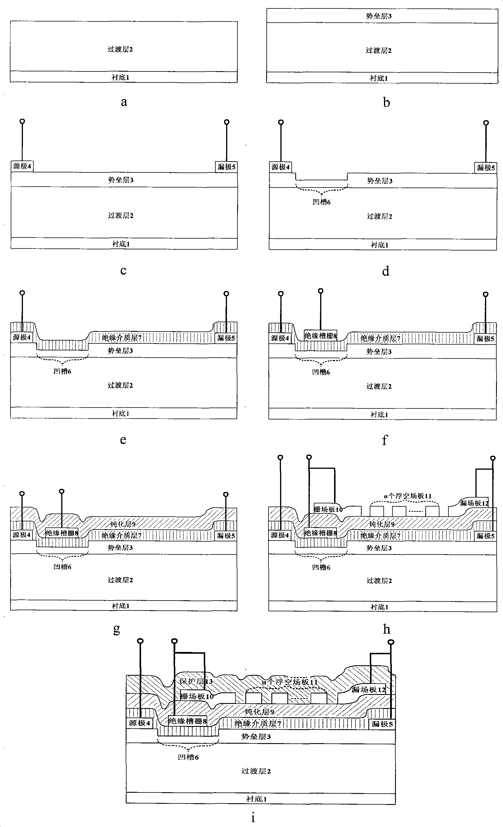
Examples
Embodiment 1
[0056] The production substrate is sapphire, and the insulating dielectric layer is SiO 2 , the passivation layer is SiN, the protective layer is SiN, and the grid field plate, drain field plate and each floating field plate are Ti / Au metal composite gate-drain composite field plate power devices, and the process is:
[0057] 1. Epitaxial undoped transition layer 2 with a thickness of 1 μm on the sapphire substrate 1 by metal organic chemical vapor deposition technology, the transition layer is composed of GaN materials with thicknesses of 50 nm and 0.95 μm from bottom to top. The process conditions used for the epitaxial lower layer GaN material are: temperature 550°C, pressure 155 Torr, hydrogen gas flow rate 5500 sccm, ammonia gas flow rate 5500 sccm, gallium source flow rate 50 μmol / min; the process conditions for the epitaxial upper layer GaN material are: temperature 1090°C, pressure 155 Torr, hydrogen flow rate 5500 sccm, ammonia gas flow rate 5500 sccm, gallium source ...
Embodiment 2
[0067] The production substrate is silicon carbide, the insulating dielectric layer is SiN, and the passivation layer is SiO 2 , the protective layer is SiO 2 , the grid field plate, the drain field plate and each floating field plate are Ni / Au metal composite gate-drain composite field plate power devices, and the process is:
[0068] 1. An undoped transition layer 2 with a thickness of 2.8 μm is epitaxially formed on a silicon carbide substrate 1 by metal-organic chemical vapor deposition technology. Made of GaN material. The process conditions used for the epitaxial lower layer AlN material are: temperature 1020°C, pressure 160 Torr, hydrogen gas flow rate 4700 sccm, ammonia gas flow rate 4700 sccm, aluminum source flow rate 11 μmol / min; the process conditions for the epitaxial upper layer GaN material are: temperature 1020°C, pressure 160 Torr, hydrogen flow rate 4700 sccm, ammonia gas flow rate 4700 sccm, gallium source flow rate 150 μmol / min.
[0069] 2. Deposit undop...
Embodiment 3
[0078] The production substrate is silicon, and the insulating dielectric layer is Al 2 o 3 , the passivation layer is SiN, the protective layer is SiN, the gate field plate, the drain field plate and each floating field plate are a gate-drain composite field plate power device composed of Pt / Au metal, and the process is:
[0079] 1. Using metal organic chemical vapor deposition technology to epitaxially undoped transition layer 2 with a thickness of 5 μm on the silicon substrate 1, the transition layer is composed of AlN material with a thickness of 120 nm and GaN material with a thickness of 4.88 μm from bottom to top constitute. The process conditions used for the epitaxial lower layer AlN material are: temperature 850 ° C, pressure 158 Torr, hydrogen gas flow rate 4800 sccm, ammonia gas flow rate 4800 sccm, aluminum source flow rate 33 μmol / min; the process conditions used for the epitaxial upper layer GaN material are: temperature 1040°C, pressure 158 Torr, hydrogen flo...
PUM
| Property | Measurement | Unit |
|---|---|---|
| Thickness | aaaaa | aaaaa |
| Length | aaaaa | aaaaa |
| Length | aaaaa | aaaaa |
Abstract
Description
Claims
Application Information