Buffer amplifier for source driver

a buffer amplifier and source driver technology, applied in the direction of dc-amplifiers with dc-coupled stages, amplifiers with semiconductor devices/discharge tubes, differential amplifiers, etc., can solve the problem of large chip layout area consumed by the footprint of the amplifier structure, inequal charge rate and discharge rate of the output stage, and inaccurate voltage levels. to achieve the effect of reducing power consumption

Inactive Publication Date: 2008-03-25
DENMOS TECH
View PDF7 Cites 16 Cited by
  • Summary
  • Abstract
  • Description
  • Claims
  • Application Information

AI Technical Summary

Benefits of technology

[0009]Accordingly, the present invention is directed to provide a buffer amplifier for source driver, which is able to reduce power consumption during use in output buffer amplifier.
[0011]According to yet another aspect of the present invention, a buffer amplifier for source driver is provided, which allows for the charge rate and the discharge rate of the output stage to be equal.
[0015]According to the present invention, an N-type differential amplifier and a P-type differential amplifier are used as the input stages, and a class AB amplifier is used to push-pull the output stage structure, so that rail-to-rail input / output can be achieved by the present invention. The output stage of the buffer amplifier in the present invention possesses such characteristics as higher charge / discharge capability, faster speed, and equal charge / discharge time. Moreover, the buffer amplifier in the present invention has advantages such as lower power consumption, higher slew rate, and a more stable output.

Problems solved by technology

However, a larger chip layout area will be consumed by the footprint of the amplifier structure of the aforementioned patent when used as the output buffer.
However, the gate of the output NMOSFET (N-type metal oxide semiconductor field effect transistor) in the aforementioned circuit is coupled to a constant bias, which results in an inequality between the charge rate and the discharge rate of the output stage.
If the aforementioned circuit is used as a reference voltage generator in a source driver inside a plurality of amplifiers A101 in the circuit shown in FIG. 1, inaccurate voltage levels may be resulted.
Moreover, DC power is consumed regularly because the gate of the output NMOS in the circuit is coupled to a constant bias.

Method used


Image

  • Buffer amplifier for source driver
  • Buffer amplifier for source driver
  • Buffer amplifier for source driver

Examples


Embodiment Construction

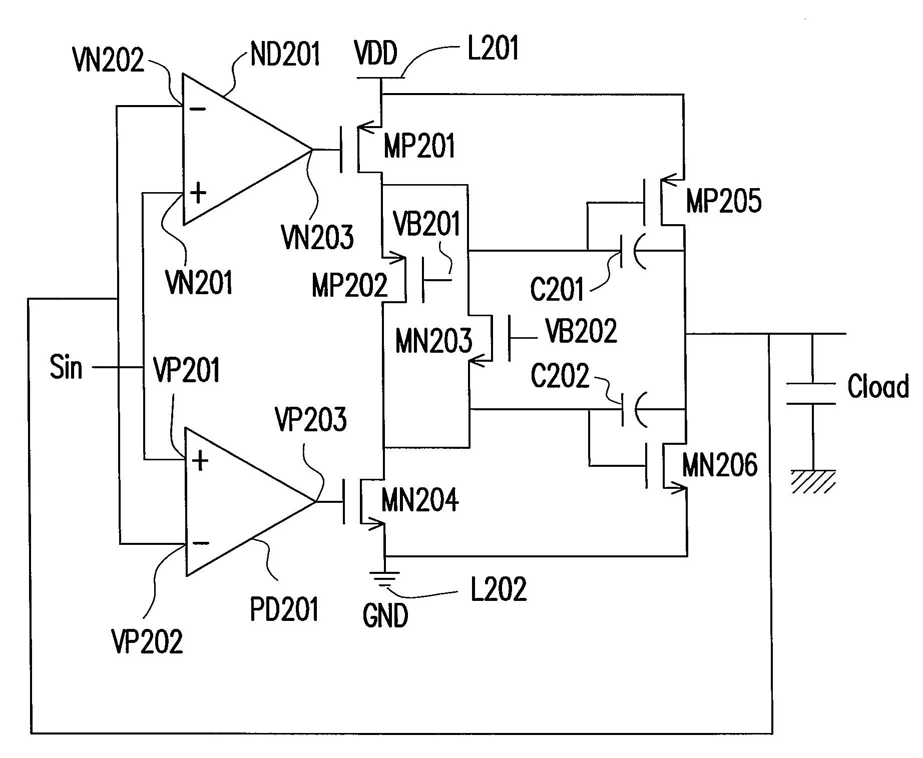
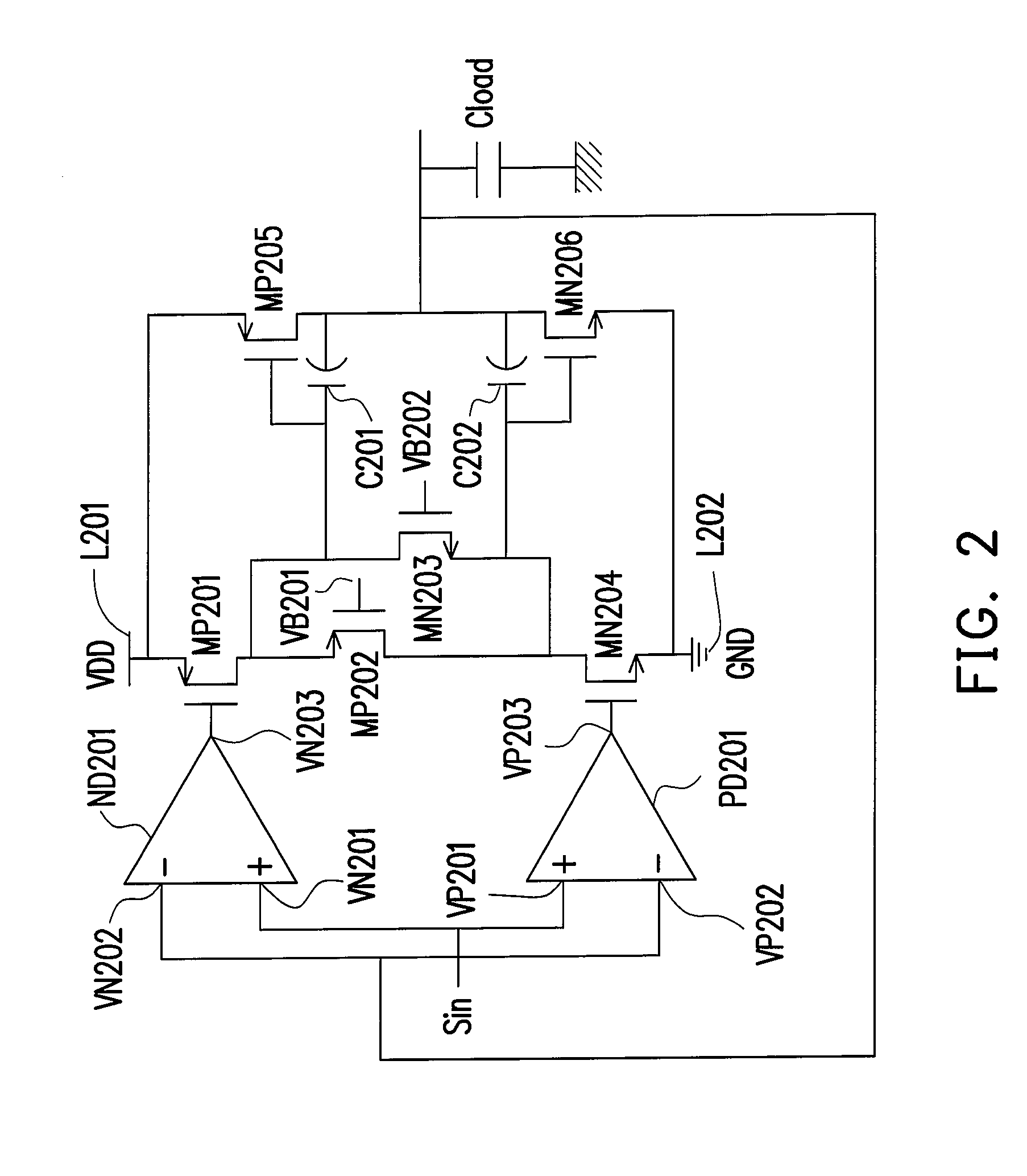
[0026]FIG. 2 is a circuit diagram of a buffer amplifier for source driver according to an embodiment of the present invention. Referring to FIG. 2, the buffer amplifier includes an N-type differential amplifier ND201, a P-type differential amplifier PD201, a 1st transistor MP201, a 2nd transistor MP202, a 3rd transistor MN203, a 4th transistor MN204, a first capacitor C201, a second capacitor C202, a 5th transistor MP205, and a 6th transistor MN206.

[0027]The N-type differential amplifier ND201 includes a positive input terminal VN201, a negative input terminal VN202, and an output terminal VN203, in which the positive input terminal VN201 is used for receiving an input signal Sin. The P-type differential amplifier includes a positive input terminal VP201, a negative input terminal VP202, and an output terminal VP203, in which the positive input terminal VP201 is used for receiving the input signal Sin, and the negative input terminal VP202 is coupled to the negative input terminal V...


PUM


Abstract

A buffer amplifier for source driver is disclosed. The buffer amplifier has an N-channel differential amplifier and a P-channel differential amplifier as its input stages so as to achieve rail-to-rail input, and a class AB amplifier to push-pull the output stage so as to achieve rail-to-rail output. The output stage of the buffer amplifier is capable of larger charge / discharge, is faster, and has equal charge / discharge time. More importantly, the buffer amplifier has advantages such as lower power consumption, higher slew rate, and a more stable output.

Description

CROSS-REFERENCE TO RELATED APPLICATION[0001]This application claims the priority benefit of Taiwan application serial no. 94145028, filed on Dec. 19, 2005. All disclosure of the Taiwan application is incorporated herein by reference.BACKGROUND OF THE INVENTION[0002]1. Field of Invention[0003]The present invention relates to an amplifier for source driver. More particularly, the present invention relates to a buffer amplifier for source driver.[0004]2. Description of Related Art[0005]Nowadays, flat panel displays, for example, such as LCD, have been used widely. Along with the improvement of the semiconductor technology, LCD is known to have such advantages as lower power consumption, smaller size and lighter weight, higher resolution, higher color saturation, and longer lifespan. Thus, LCD is widely applied to electronic products related to our daily lives, such as the use of LCD screens in laptop computers or desktop computers and LCD TVs. In which, the source driver is a critical ...

Claims


Application Information

Patent Timeline
Patent Type & Authority Patents(United States)
IPC IPC(8): H03F3/45
CPCH03F3/45183H03F2203/45684
Inventor HUANG, CHUN-CHIN
Owner DENMOS TECH
Why Eureka
Try Eureka