Waveguide design incorporating reflective optics

a waveguide and optics technology, applied in waveguides, optical elements, instruments, etc., can solve the problems of large dn/dt, difficult positioning of the receive side waveguide, and complicated manufacturing process of the discrete beam cas

Inactive Publication Date: 2008-04-01
ZETTA RES & DEV LLC RPO SERIES
View PDF6 Cites 97 Cited by
  • Summary
  • Abstract
  • Description
  • Claims
  • Application Information

AI Technical Summary

Benefits of technology

[0134]Referring to FIG. 12a, yet another advantage of the inventive approach is that during assembly, space 122 between end face 1103 and VCL 33 can be filled with adhesive to attach the VCL to the element array. This is not possible with the prior art lens approach because curved end face 31 relies on the polymer / air refractive index contrast. As will become clear below, it is preferable that the adhesive and the material used to form the transmit and receive elements are index matched, ie. their refractive indices are substantially equal.

Problems solved by technology

The discrete beam case also complicates the manufacturing process, because the receive side waveguides need to be critically aligned (in the horizontal plane) with the transmit side waveguides; with a lamina of light, the horizontal positioning of the receive side waveguides is non-critical.
However in certain applications such as the optical touch screen sensor of FIG. 1 and the transmission device of FIG. 2, a large dn / dT is disadvantageous because modest variations in ambient temperature, say over an operating range of −10 to 50° C., adversely affect the horizontal collimation at the planar lenses in FIGS. 1 and 2, by changing the angle of refraction at the polymer / air interfaces.
If the temperature drifts too far, variations in the emission angles at the transmit side and / or in the acceptance angles at the receive side will reduce the collection efficiency, representing a source of optical loss in the system.
Furthermore, stray light may be collected by adjacent receive lenses, possibly causing errors in determining the position of a touch event.
However silica glass waveguides are much more expensive to fabricate, both in terms of fabrication equipment and processing time, and are simply not an option for a mass-produced consumer electronics device such as an optical touch screen sensor.
The transmit and receive lenses of the existing optical touch screen design also encounter difficulties with collimation in the vertical plane, where for ease of assembly it is convenient to use a single VCL for all transmit or receive lenses in each array along the respective sides of the optical touch screen.
The unavoidable spread of the beam in the vertical direction is another cause of optical power loss in the prior art design.
Another difficulty arises when the substrate is introduced into the picture.
This represents yet another source of optical loss in the prior art system, and while in theory it is possible to avoid the shadowing effect by cutting the substrate in a shaped fashion, this would require extremely precise laser cutting and is simply impractical for the manufacture of low cost devices.
Yet another problem with the transmit and receive lenses of the existing design is that the curved end face must have an air / lens material interface.
However there is then a risk that the curved end face could be damaged, for example during assembly of the optical touch screen sensor.

Method used


Image

  • Waveguide design incorporating reflective optics
  • Waveguide design incorporating reflective optics
  • Waveguide design incorporating reflective optics

Examples


example 1

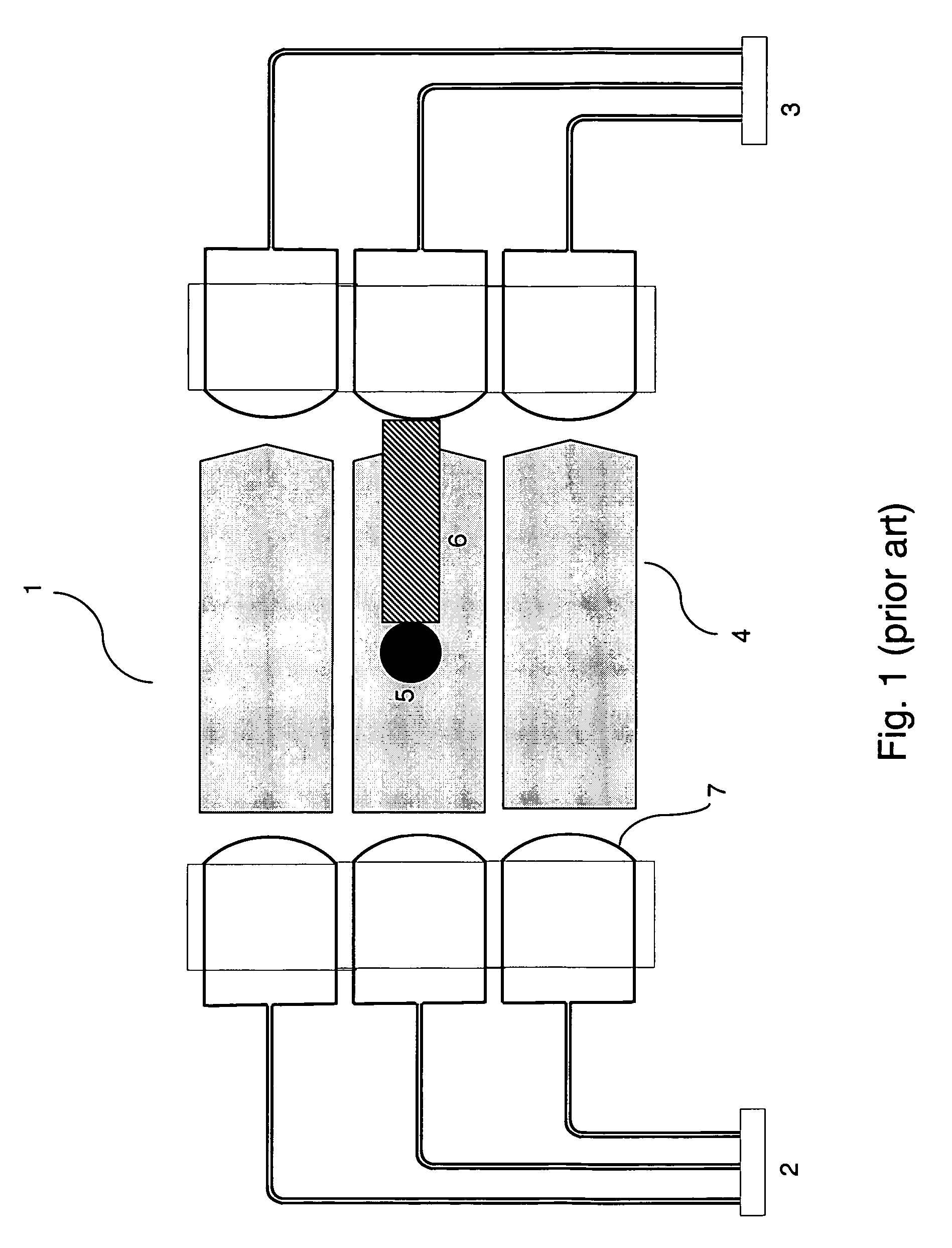
[0115]This example is designed to illustrate the temperature sensitivity of a paired set of prior art transmit and receive lenses that form part of an optical touch screen sensor. FIG. 5 shows transmit lens 50 and receive lens 51, each composed of polymer A and being mirror images of each other. In this example the lenses are assumed to be perfectly aligned in the horizontal plane, ie. that they share an optical axis 52. The width of the touch screen, ie. the tip-to-tip separation 53 of the lenses, is 65 mm, and the cylindrical lenses that collimate the beams in the vertical (out of page) dimension have been omitted for clarity. Waveguides 54 and 55 entering the ends of lenses 50 and 51 at points 502 and 503 are both 8 μm wide and aligned with the axis of symmetry of the respective lens. Each lens 50, 51 has a straight section 56 of length 1460 μm and width 57 of 750 μm, and ends in a curved surface 58, 501 that is an arc of a circle with radius of curvature 570 μm. Ideally, light 5...

example 2

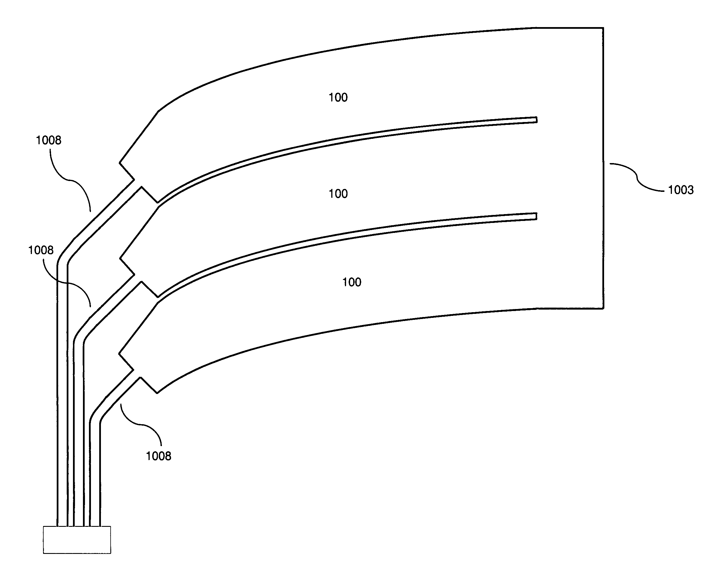
[0131]In accordance with the invention, a transmit element 100 incorporating a parabolic reflector is shown in FIG. 10. Transmit waveguide 102 guides light 101 through an angle β=33.1° at bend 1007, along straight section 1008 and into polymer slab region 103 at point 104, whereupon it spreads with divergence angle 2φ and encounters curved side 106 that is a portion of a parabola with focus at point 104 and with directrix perpendicular to optical axis 105. The angle of incidence θi ranges from 63° at point 107 to 68° at point 108, and is always greater than the critical angle (see Table 4) so that the total internal reflection condition is satisfied. After reflecting off curved side 106, the light is collimated along optical axis 105. Straight sides 109, 1000 and 1001 of polymer slab region 103 are 204 μm, 687 μm and 220 μm long, and curved sides 1002 and 106 are both 3493 μm long. After reflection off curved side 106, the light is collimated into parallel rays 1009 that exit transm...

example 3

[0136]A transmit element 150 incorporating an elliptical reflector and designed for a 65 mm wide touch screen is shown in FIG. 15. Transmit waveguide 152 guides light 151 through an angle β=33.1° at bend 1507, along straight section 1508 and into polymer slab region 153 at point 154, whereupon it spreads with divergence angle 2φ and encounters curved side 156 that is a segment of an ellipse with one focus at point 154 and the other focus at point 1504 located a distance 32.5 mm from end face 1503. The angle of incidence θi ranges from 63° at point 157 to 68° at point 158, and is always greater than the critical angle (see Table 4) so that the total internal reflection condition is satisfied. Straight sides 159, 1500 and 1501 of polymer slab region 153 are 204 μm, 687 μm and 220 μm long, and curved sides 1502 and 156 are both 3493 μm long. After reflection off curved side 156, the light is focused into a beam 1509 that exits transmit element 150 at end face 1503 and converges to poin...


PUM


Abstract

This invention relates to devices for coupling light between an optical waveguide and an optical element in a manner that is substantially independent of temperature, using reflective optics. Certain embodiments of the invention concern improved designs for the transmit and receive optics of a waveguide-based optical touch screen sensor, incorporating reflective optics. The improved designs have substantially temperature independent operation and reduced optical losses. In one preferred embodiment the improved design incorporates a parabolic or quasi-parabolic reflector. In another preferred embodiment the improved design incorporates an elliptical or quasi-elliptical reflector. The transmit and receive elements and associated waveguides preferably comprise photo-patternable polymers.

Description

FIELD OF INVENTION[0001]This invention relates to an improved design for the transmit and receive optics of a waveguide-based optical touch screen sensor. The improved design incorporates reflective optics, and has the advantages of reduced temperature sensitivity and reduced optical losses. However, it will be appreciated that the invention is not limited to this particular field of use, and may be applied to the coupling of light between any two optical elements, at least one of which is a waveguide.BACKGROUND OF INVENTION[0002]Any discussion of the prior art throughout the specification should in no way be considered as an admission that such prior art is widely known or forms part of common general knowledge in the field.[0003]FIG. 1 illustrates the operation of an optical touch screen sensor 1 described in U.S. Pat. Nos. 5,914,709, 6,181,842 and 6,351,260, and US Patent Application Nos. 2002 / 0088930 A1 and 2004 / 0201579 A1 (the contents of which are incorporated into this specif...

Claims


Application Information

Patent Timeline
Patent Type & Authority Patents(United States)
IPC IPC(8): G02B6/10G06F3/042
CPCG02B6/122G02B6/1221G02B6/32G02B6/4298G06F3/0421H01P3/00G02B6/38
Inventor CHARTERS, ROBBIECORNISH, BENJAMINLUTHER-DAVIES, BARRYKUKULJ, DAXATKINS, GRAHAM
Owner ZETTA RES & DEV LLC RPO SERIES
Why Eureka
Try Eureka