Printed wiring board and electronic device using the same
a wiring board and electronic device technology, applied in the direction of conductive pattern formation, electrical apparatus construction details, semiconductor/solid-state device details, etc., can solve problems such as deterioration phenomena, electrical leakage or short circuit between wirings
- Summary
- Abstract
- Description
- Claims
- Application Information
AI Technical Summary
Benefits of technology
Problems solved by technology
Method used
Image
Examples
embodiment 1
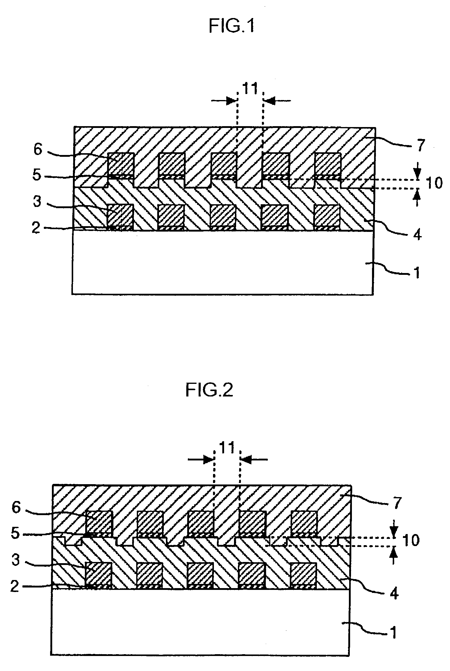
[0066]FIG. 1 is a schematic cross-sectional view of a printed wiring board of the present embodiment. The upper part of an insulating resin layer 4 existing in spaces 11 between metal conductors (wiring) was formed at a position lower than the boundary face between the under surface of a base metal layer 5 and the upper face of the insulating resin layer 4, and a protective insulating layer 7 was formed on the top thereof.
[0067]Namely, the interface between the protective insulating layer 7 and the insulating resin layer 4 existing in spaces 11 between metal conductors (wiring) was at a lower position by a level difference 10 than the boundary face between the base metal layer 5 and the insulating resin layer 4.
[0068]FIG. 13 is an additional process chart including additional processes taking place after process (k) of a conventional process shown in FIG. 12 so that the upper portion of the insulating resin layer 4 existing in spaces 11 between metal conductors was made at a lower p...
embodiment 2
[0072]FIG. 2 is a schematic cross-sectional view of a printed wiring board of this embodiment. A central part of an upper face of an insulating resin layer 4 existing in spaces between metal conductors 11 was removed by ion beam processing so as to be lower than the boundary face between a base metal layer 5 and the insulating resin layer 4, and a protective insulating layer 7 was formed on the top thereof.
[0073]A part of the interface between the protective insulating layer 7 and the insulating resin layer 4 existing in spaces 11 between metal conductors (wiring) was provided at a lower position by a level difference 10 than the boundary face between the base metal layer 5 and the insulating resin layer 4. Here, the level difference 10 was approximately 500 nm.
embodiment 3
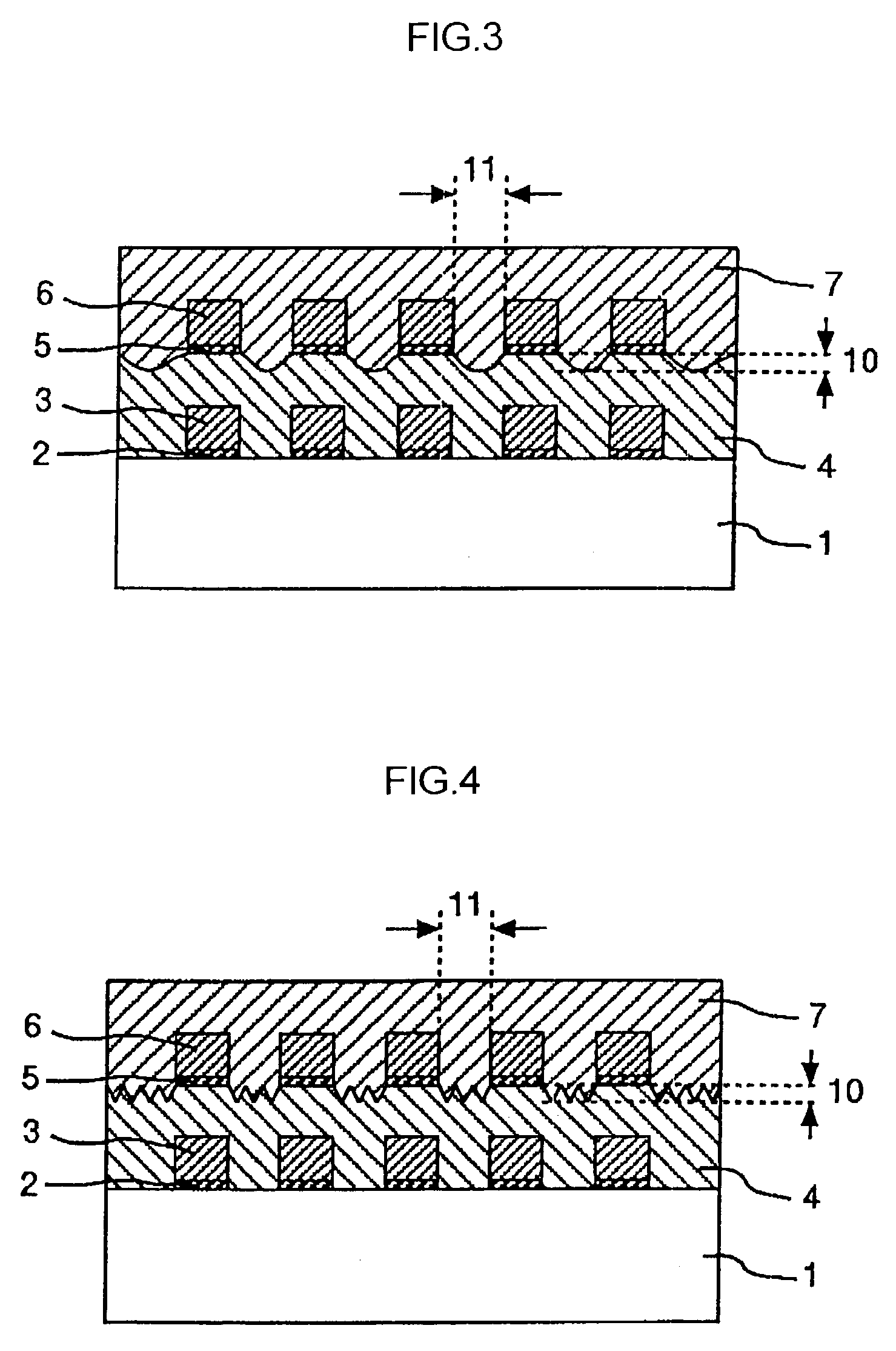
[0074]FIG. 3 is a schematic cross-sectional view of a printed wiring board of this embodiment. A central part of an upper face of an insulating resin layer 4 existing in spaces 11 between metal conductors was removed and formed in a concave shape by a laser processing. The bottom of the concave portion was formed at a position lower than the boundary face between the base metal layer 5 and the insulating resin layer 4, and a protective insulating layer 7 was formed on the top thereof.
[0075]A concave-shaped interface between the protective insulating layer 7 and the insulating resin layer 4 existing in spaces between the metal conductors (wiring) was provided at a lower position by a level difference 10 than the boundary face between the base metal layer 5 and the insulating resin layer 4. Here, the level difference 10 was approximately 1 μm.
PUM
 Abstract
Description
Claims
Application Information
 - R&D
- Intellectual Property
- Life Sciences
- Materials
- Tech Scout
- Unparalleled Data Quality
- Higher Quality Content
- 60% Fewer Hallucinations
Browse by: Latest US Patents, China's latest patents, Technical Efficacy Thesaurus, Application Domain, Technology Topic, Popular Technical Reports.
© 2025 PatSnap. All rights reserved.Legal|Privacy policy|Modern Slavery Act Transparency Statement|Sitemap|About US| Contact US: help@patsnap.com


