Post passivation interconnection process and structures

a post-passivation and interconnection technology, applied in the direction of electrical apparatus, semiconductor devices, semiconductor/solid-state device details, etc., can solve the problems of increasing negative impact on circuit performance, significantly degrading chip performance, and large size of analog circuitry, so as to improve the rf performance of high-performance integrated circuits

Active Publication Date: 2008-04-08
QUALCOMM INC
View PDF14 Cites 31 Cited by
  • Summary
  • Abstract
  • Description
  • Claims
  • Application Information

AI Technical Summary

Benefits of technology

[0021]It is the primary objective of the invention to improve the RF performance of High Performance Integrated Circuits.

Problems solved by technology

One of the major challenges in the creation of analog processing circuitry (using digital processing procedures and equipment) is that a number of the components that are used for analog circuitry are large in size and are therefore not readily integrated into devices that typically have feature sizes that approach the sub-micron range.
The main components that offer a challenge in this respect are capacitors and inductors, since both these components are, for typical analog processing circuits, of considerable size.
The metal connections which connect the Integrated Circuit to other circuit or system components become of relative more importance and have, with the further miniaturization of the IC, an increasingly negative impact on circuit performance.
The parasitic capacitance and resistance of the metal interconnections increase, which degrades the chip performance significantly.
Attempts to reduce the resistance by using wider metal lines result in higher capacitance of these wires.
It is technically difficult and economically expensive to create thicker than 2 μm aluminum metal lines due to the cost and stress concerns of blanket sputtering.
Electroplating the whole wafer with thick metal creates large stress and carries a very high material (metal) cost.
Furthermore, the thickness of damascene copper is usually defined by the insulator thickness, typically chemical vapor deposited (CVD) oxides, which does not offer the desired thickness due to stress and cost concerns.
Again it is also technically difficult and economically expensive to create thicker than 2 μm copper lines.
The current fine-line techniques, either using sputtered aluminum or damascene copper, cannot provide inductors with a high quality factor due to the high resistance of fine-line metals.
The resistance of the metal traces used to form the inductor coils will consume electrical energy.
In addition, the fine-line techniques further imply close physical proximity between the created inductor and the surface of the substrate over which the inductor has been created (typically less than 10 μm), resulting in high electro-magnetic losses in the silicon substrate which in turn further results in reducing the Q value of the inductor.

Method used


Image

  • Post passivation interconnection process and structures
  • Post passivation interconnection process and structures
  • Post passivation interconnection process and structures

Examples


Embodiment Construction

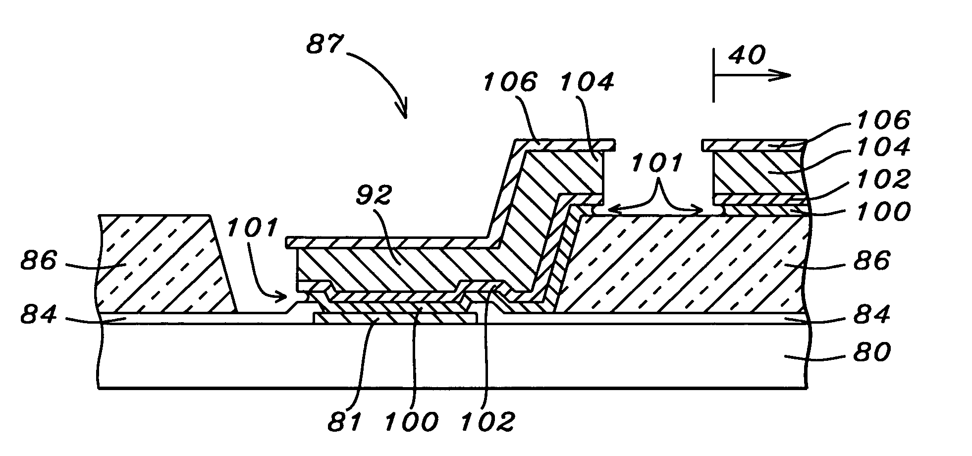
[0045]The post-passivation process, described in U.S. Pat. Nos. 6,383,916 and 6,495,442, to the same inventor as the current invention, teaches an Integrated Circuit structure where re-distribution and interconnect metal layers are created in layers of dielectric over the passivation layer of a conventional Integrated Circuit (IC). A layer of passivation is deposited over the IC, a thick layer of polymer is alternately deposited over the surface of the layer of passivation, and thick, wide metal lines are formed over the passivation.

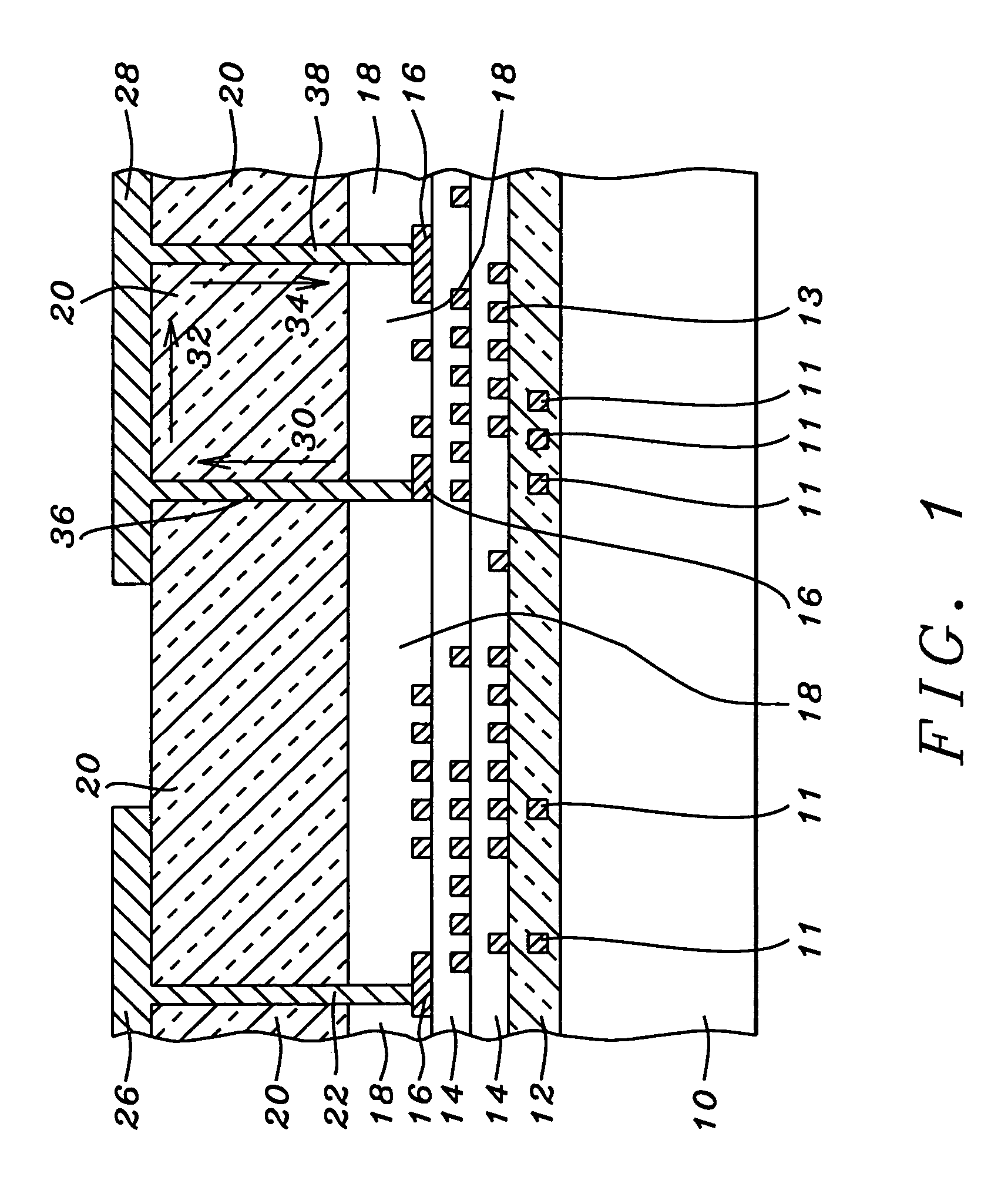
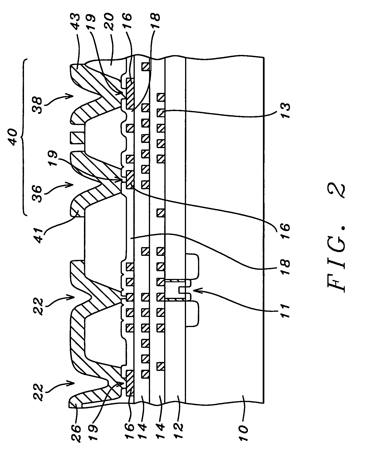
[0046]U.S. Pat. No. 6,303,423 and the co-pending related patent applications, also assigned to a common assignee as the current invention, address, among other objectives, the creation of an inductor whereby the emphasis is on creating an inductor of high Q value above the passivation layer of a semiconductor substrate. The high quality of the inductor of the invention allows for the use of this inductor in high frequency applications while incurring min...


PUM

PropertyMeasurementUnit
thicknessaaaaaaaaaa
thicknessaaaaaaaaaa
thicknessaaaaaaaaaa

Abstract

A system and method for forming post passivation metal structures is described. Metal interconnections and high quality electrical components, such as inductors, transformers, capacitors, or resistors are formed on a layer of passivation, or on a thick layer of polymer over a passivation layer.

Description

[0001]This application is a continuation-in-part of MEG-04-013, Ser. No. 10 / 937,543, filed on Sep. 9, 2004.RELATED PATENT APPLICATIONS[0002]This application is related to MEG00-008CBBC, Ser. No. 10 / 303,451, filed on Nov. 25, 2002, MEG02-016, Ser. No. 10 / 445,558, filed on May 27, 2003, MEG02-017, Ser. No. 10 / 445,559, filed on May 27, 2003, and MEG02-018, Ser. No. 10 / 445,560, filed on May 27, 2003, all assigned to a common assignee, and all are herein incorporated by reference in their entirety.BACKGROUND OF THE INVENTION[0003]1. Field of the Invention[0004]The invention relates to the manufacturing of high performance, high current, low power, and / or low voltage Integrated Circuit (IC's), and, more specifically, to methods of creating high performance, high current, low power, and / or low voltage electrical components on the surface of a semiconductor substrate.[0005]2. Description of the Related Art[0006]The continued emphasis in the semiconductor technology is to create improved per...

Claims


Application Information

Patent Timeline
Patent Type & Authority Patents(United States)
IPC IPC(8): H01L29/72
CPCH01L23/3171H01L23/5223H01L23/5227H01L23/5228H01L23/5329H01L24/05H01L24/13H01L2224/0401H01L2224/04042H01L2224/13022H01L2224/131H01L2224/13144H01L2924/04953H01L2924/05042H01L2924/14H01L2924/19015H01L2924/19041H01L2924/19042H01L2924/19043H01L2924/19104H01L2924/30105H01L2924/014H01L2924/01019
Inventor LIN, MOU-SHIUNGCHOU, CHIEN-KANGCHOU, CHIU-MING
Owner QUALCOMM INC
Why Eureka
Try Eureka