Fully differential sensing apparatus and input common-mode feedback circuit thereof

a technology of input common-mode feedback and sensing apparatus, which is applied in the direction of differential amplifiers, digital storage, instruments, etc., can solve the problems of reducing the situation becoming worse, so as to reduce the input impedance and output impedance, and reduce the transfer gain of this charge integration amplifier

Active Publication Date: 2008-04-15
IND TECH RES INST
View PDF4 Cites 17 Cited by
  • Summary
  • Abstract
  • Description
  • Claims
  • Application Information

AI Technical Summary

Benefits of technology

[0014]The described technique in the background of invention to add a dc path from differential amplifier's output to its input node could help to define a dc operating point at input node(s) but not suffice to restore the input common mode fast enough if the resistance value of the dc path and the feedback integration capacitor comprise a time constant that is too large to do something useful in time. Therefore, the goal of this invention is to design an input common mode feedback circuit to define a specific dc operating point for the input nodes of the differential amplifier, effectively maintain the input common mode voltage on these input nodes and to introduce negligible charge leak path for the capacitive source(s) so that net charge flow from the capacitive source(s) can be fully taken to the feedback integration capacitor.
[0015]The adaptive conductance elements and the error amplifier are designed for this purpose. When the input common mode voltage at the input nodes of the differential amplifier falls within a small tolerance away from the set value, these adaptive conductance elements are in the state of high impedance and the capacitive source(s) sees no extra charge leak path. The high impedance state and the capacitive source can constitute a high pass corner at a very low frequency so that transfer gain at low frequency baseband won't be hurt at all. When the input common mode voltage at the input nodes of the differential amplifier starts to deviate out of a small range from the set value, these adaptive conductance elements will be turned into a low impedance state, making the input common mode feedback circuit a negative feedback loop to fast restore the error to nearly a zero value and then turned into high impedance state again. It is also worthwhile our suggesting attention that dc offset very often should be carefully taken care of within the differential amplifier itself for a typical charge integration amplifier to ensure that the differential amplifier can work at correct operating point.

Problems solved by technology

This can cause unwanted charge leak to the parasitic capacitance between the capacitive sources and the input nodes of the differential amplifier, and reduce the transfer gain of this charge integration amplifier.
This situation becomes worse when the modulated biasing voltage is applied to the capacitive sources.

Method used


Image

  • Fully differential sensing apparatus and input common-mode feedback circuit thereof
  • Fully differential sensing apparatus and input common-mode feedback circuit thereof
  • Fully differential sensing apparatus and input common-mode feedback circuit thereof

Examples


Embodiment Construction

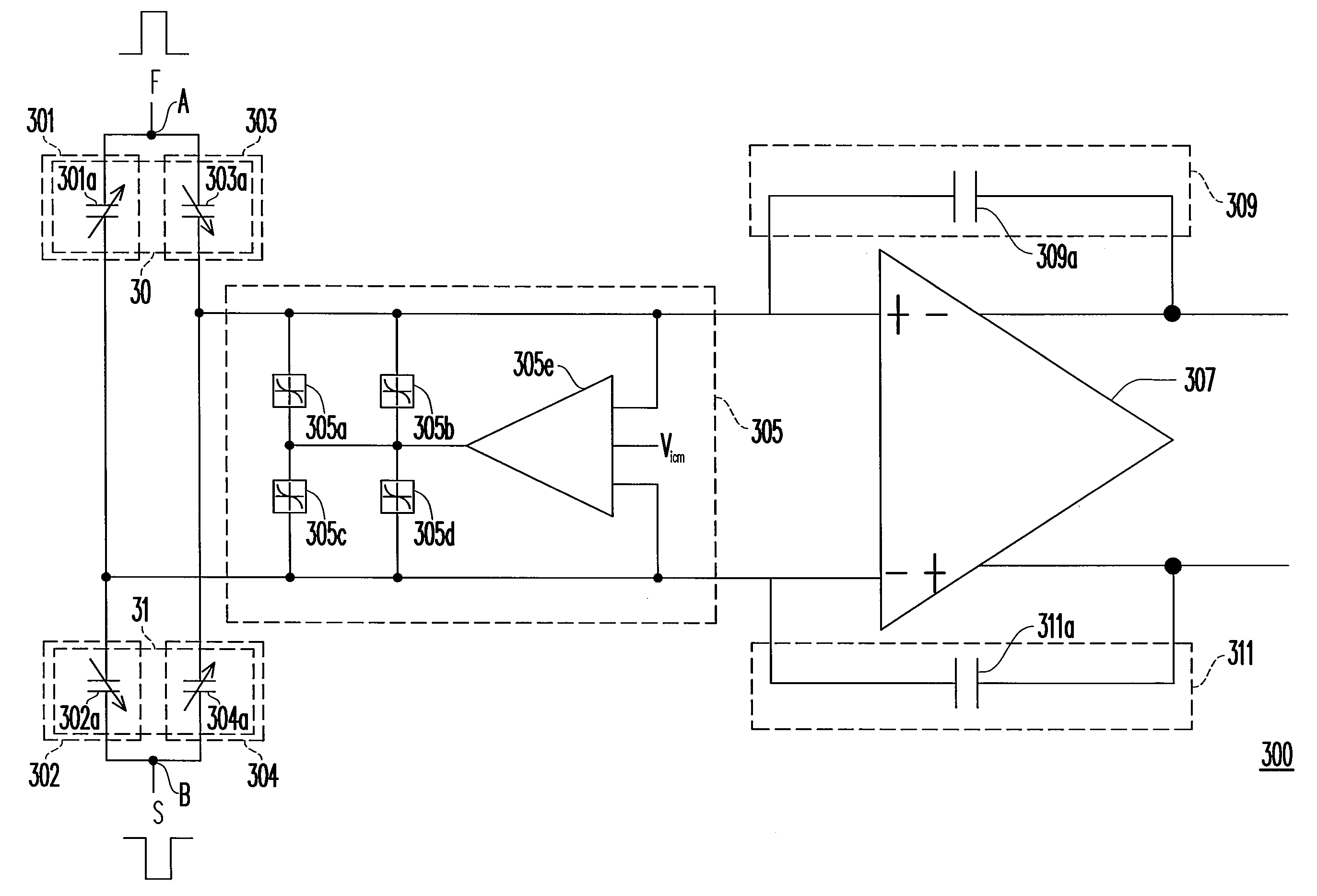
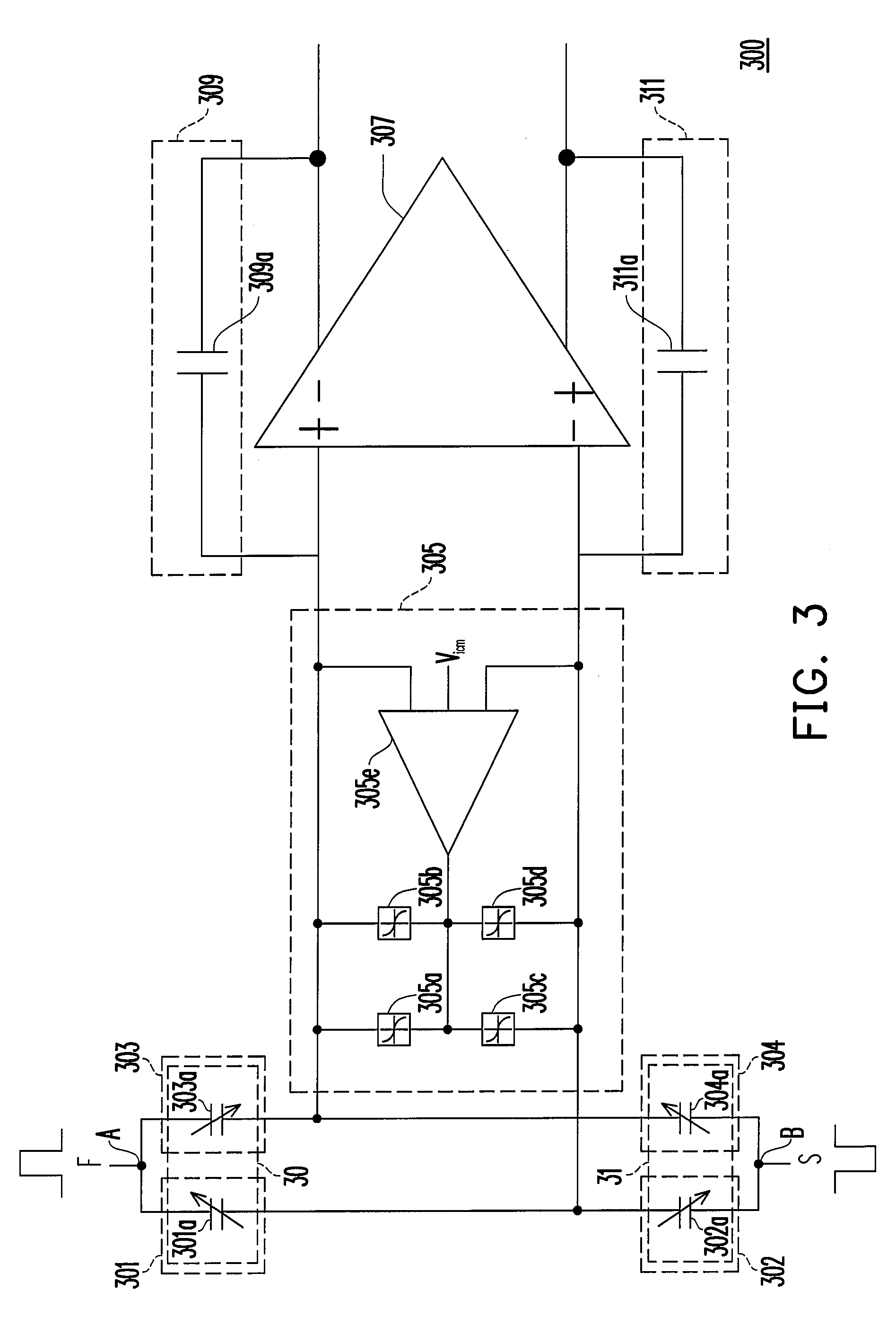
[0027]The following description is provided to explain some applicable usage of current invention. Various modifications and other alterations in the structure and method of operations within the spirit and scope of this invention, however, will remain apparent to those skilled in the art, since the problems to solve and principles to use have been defined and explained within this invention. FIG. 3 is a circuit diagram of a fully differential sensing apparatus based on an embodiment of the present invention. Referring to FIG. 3, a fully differential sensing apparatus 300 includes a first input impedance 301, a second input impedance 303, an input common-mode feedback (ICMFB) circuit 305, a fully differential amplifier 307, a first feedback impedance 309, and a second feedback impedance 311. In the present embodiment, the fully differential sensing apparatus 300 may further include third input impedance 302 and fourth input impedance 304. It should be noted that the present inventio...


PUM


Abstract

A fully differential sensing apparatus and an input common mode feedback circuit are provided. The input common mode feedback circuit includes a common mode error amplifier and a plurality of adaptive conductance elements. Each adaptive conductance element behaves with a low impedance characteristic when its anode voltage is greater than its cathode voltage by a positive threshold voltage or, on the contrary, when the anode voltage of such an adaptive conductance element is lower than its cathode voltage by a negative threshold voltage, the adaptive element also behaves with a low impedance characteristic; otherwise the aforementioned adaptive conductance element behaves with a high impedance characteristic. The common mode error amplifier and a plurality of such adaptive conductance elements form a negative feedback loop to effectively maintain the input common voltage of a fully differential input amplifier, which can be used for a fully differential sensing apparatus.

Description

CROSS-REFERENCE TO RELATED APPLICATION[0001]This application claims the priority benefit of Taiwan application serial no. 95118210, filed on May 23, 2006. All disclosure of the Taiwan application is incorporated herein by reference.BACKGROUND OF THE INVENTION[0002]1. Field of Invention[0003]The present invention relates to a circuit for maintaining the input common-mode voltage of a differential input amplifier, and more particularly, to an input common-mode feedback circuit applicable to a differential input amplifier and a fully differential sensing apparatus applying the aforementioned input common-mode feedback circuit.[0004]2. Description of the Related Art[0005]In the field of capacitive sensing applications, the sensed parameters can be dielectric constant, capacitance gap distance or capacitance area. Very often at least one of these parameters changes corresponding to an external stimulus. The sensed stimulus (for example, physical quantities such as pressure, movement or d...

Claims


Application Information

Patent Timeline
Patent Type & Authority Patents(United States)
IPC IPC(8): H03F3/45
CPCG11C7/062H03F1/34H03F3/393H03F3/45475H03F3/45928H03F2200/213H03F2200/264H03F2203/45078H03F2203/45101H03F2203/45134H03F2203/45138H03F2203/45424H03F2203/45512H03F2203/45586H03F2203/45588
Inventor SHIA, TIM K.CHUNG, CHI-CHENCHANG, LONG-XI
Owner IND TECH RES INST
Why Eureka
Try Eureka