Circuit and method for an SRAM with reduced power consumption

a technology of sram and power consumption, applied in the field of circuit and method of sram with reduced power consumption, can solve the problems of threshold voltage (vt) mismatch, certain dominant problematic effects, and less attractive data memory types in some respects, and achieve the effects of reducing voltage, reducing power consumption, and increasing supply voltag

Active Publication Date: 2008-04-15
TAIWAN SEMICON MFG CO LTD
View PDF7 Cites 21 Cited by
  • Summary
  • Abstract
  • Description
  • Claims
  • Application Information

AI Technical Summary

Benefits of technology

[0022]These and other problems are generally solved or circumvented, and technical advantages are generally achieved, by embodiments of the present invention, which provide circuits and methods of forming an SRAM block for use in an integrated circuit which solves the Vcc, minimum problem described above by providing a reduced voltage to the peripheral circuitry associated with the SRAM block, providing a higher supply voltage to the SRAM cell array during active cycles, and providing a level shifter circuit to supply the higher supply voltage during active cycles. The level shifter circuitry is a simple circuit that requires only 2% additional area over the existing circuitry. The power saved by operating the peripheral circuitry at the lower level is significant, estimated at 15% power savings for a typical current semiconductor process node. The SRAM block may be implemented with sleep or power down modes, stand-by modes, and active modes, by varying the voltage supplied as an input to the level shifter, the level shifter will output a high supply voltage to the array of SRAM cells only when needed, this selection is logically based on the supply voltage supplied to the peripheral circuitry.

Problems solved by technology

Dynamic memory offers excellent density and minimum required silicon area, however the need to frequently refresh the storage cells, and the loss of the stored data on power loss, makes this type of data memory less attractive in some respects, particularly for battery operated devices.
As the scaling of the dimensions of CMOS integrated circuitry gets smaller, certain dominant problematic effects such as the threshold voltage (Vt) mismatch occur including increased sub threshold leakage currents.
These effects cause the minimum supply voltage Vcc required to correctly store and retrieve data in an embedded SRAM array (usually called “Vcc, min”) to become a critical supply voltage limit.
This in turn leads to undesirably larger power consumption, especially during stand-by cycles when the SRAM is not being actively operated.
Thus the power consumption in these embedded SRAM memories is particularly important, and there is an ongoing need to reduce the power used in these SRAM memory blocks to as low a level as possible.
This higher supply voltage increases the SRAM cell static noise margin (SNM) to acceptable levels that are not otherwise possible with the lower supply voltage.
This prior art approach thus adds silicon area to the SRAM array and to the peripheral circuitry, which is undesirable as it reduces the amount of storage that can be provided in the embedded SRAM for a given application.
There is also the speed concern for the prior art reduced power design.
Due to the fact that CVDD will change from high to low from read to write operations, and VCC will change from low to high for the read to write operation, the SRAM array speed is limited, to wait for these voltage states to change.
The SRAM speed / current will also be reduced to around 40%, this is undesirable.

Method used


Image

  • Circuit and method for an SRAM with reduced power consumption
  • Circuit and method for an SRAM with reduced power consumption
  • Circuit and method for an SRAM with reduced power consumption

Examples


Embodiment Construction

[0038]The making and using of the presently preferred embodiments are discussed in detail below. It should be appreciated, however, that the present invention provides many applicable inventive concepts that can be embodied in a wide variety of specific contexts. The specific embodiments discussed are merely illustrative of specific ways to make and use the invention, and do not limit the scope of the invention.

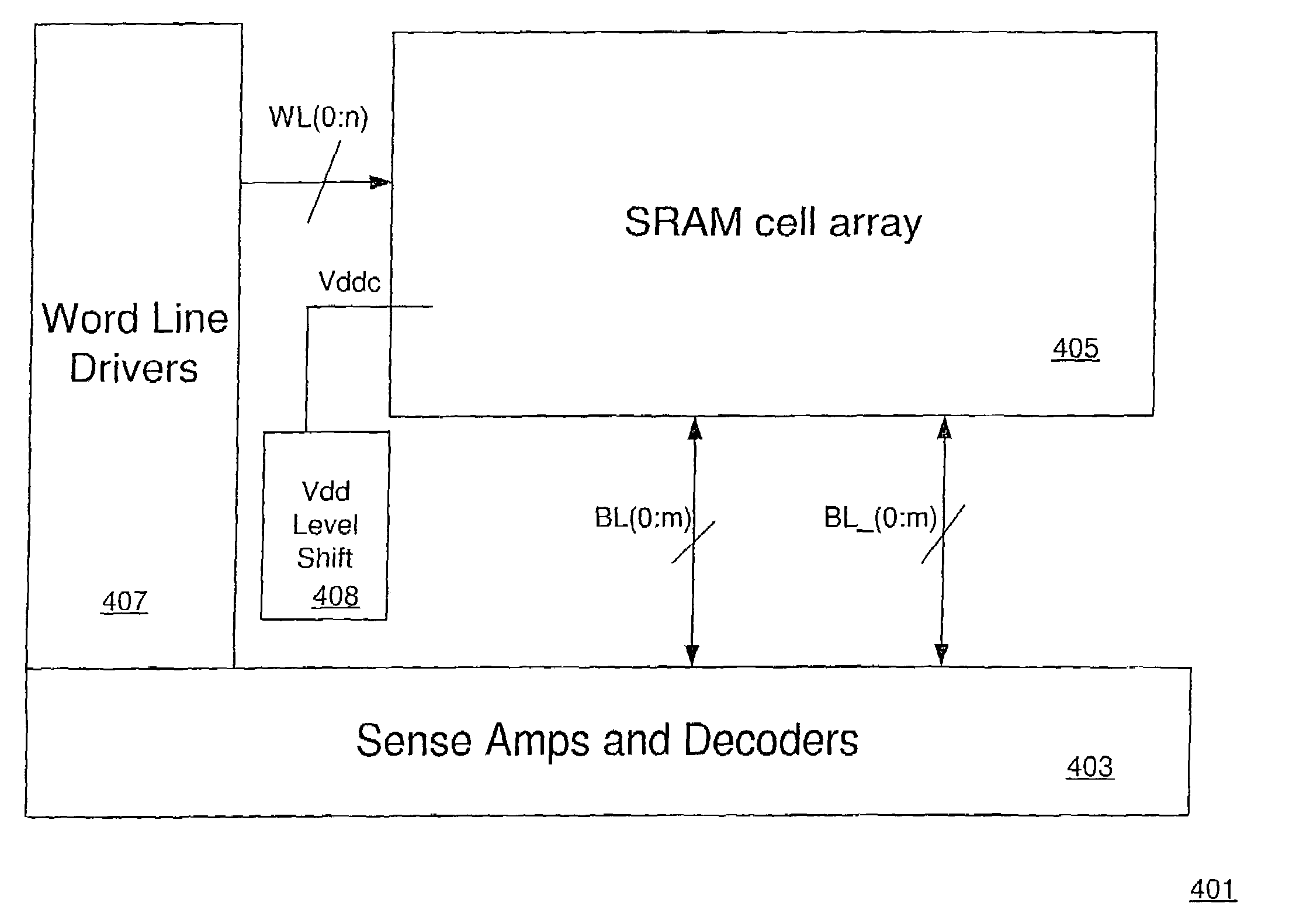
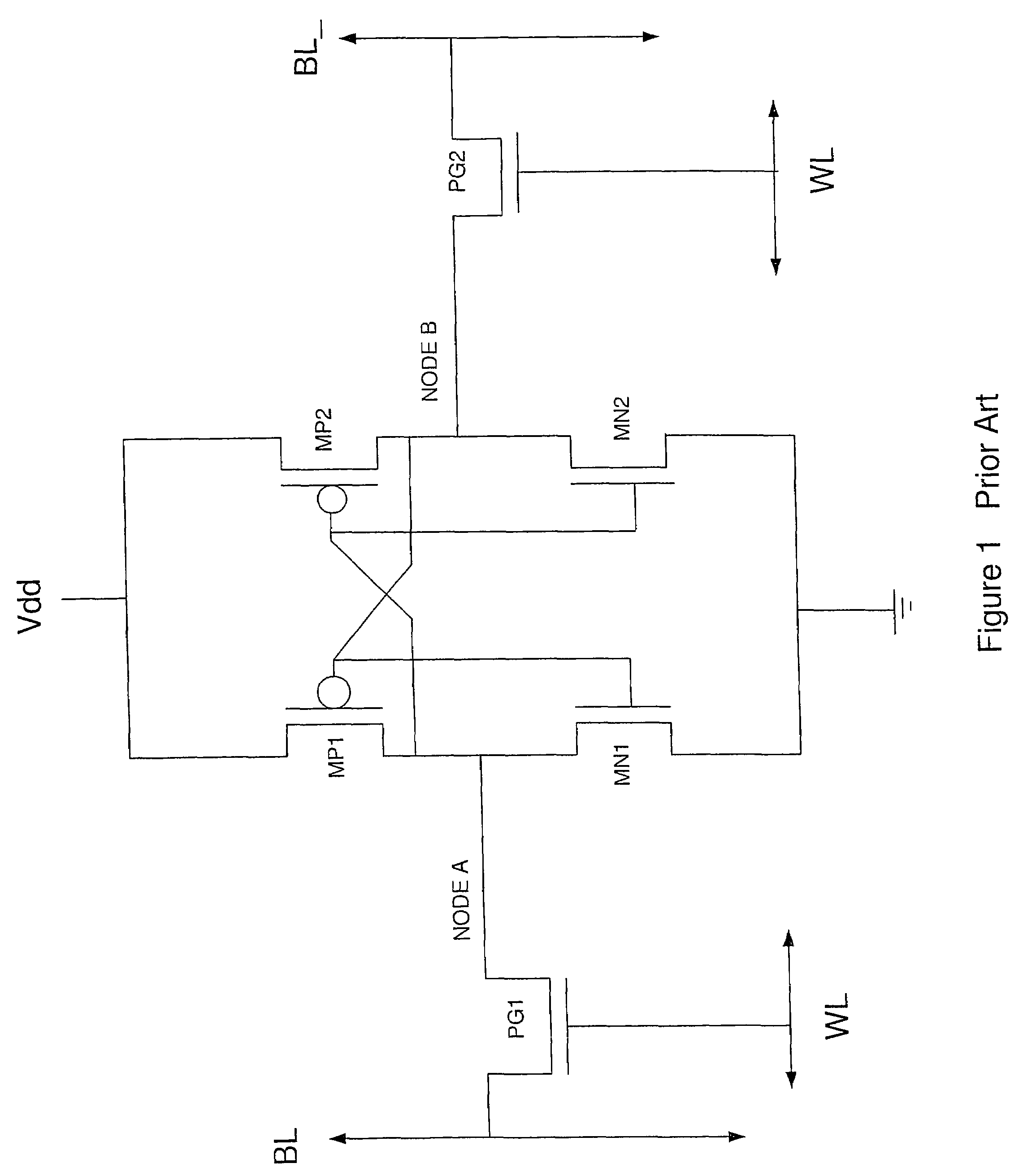
[0039]FIG. 4 depicts in a simple plan view, the major blocks of an SRAM array 401 incorporating the reduced power approach of the invention. Sense amps and decoders 403 are provided and are coupled to complementary bit lines BL (0:m) and BL_(0:m), which define columns (or rows) in SRAM cell array 405. Word line drivers 407 provide decoding and drive a selected word line for a read, write operation, the word lines WL (0:n) defining rows (or columns) in SRAM cell array 405. There is an SRAM cell at each word line, bit line intersection that may be a 6T SRAM cell as depicted in ...


PUM


Abstract

A circuit and method for providing an SRAM memory with reduced power consumption, the SRAM memory particularly useful for embedding SRAM memory with other logic and memory functions in an integrated circuit. A lower supply voltage is provided to the peripheral circuitry for the SRAM memory. A level shifter circuit is provided coupled to the lower power supply and outputting a higher supply voltage. An array of SRAM memory cells that may comprise 4T, 6T or 8T static RAM memory cells are coupled to the higher supply voltage during read and write operations. Operating the peripheral circuitry of the SRAM memory at the lower supply voltage achieves reduced power consumption for the SRAM memory and the integrated circuit.

Description

TECHNICAL FIELD[0001]The present invention relates to a circuit and method for providing a static RAM (“SRAM”) memory with reduced power consumption. This SRAM is particularly useful as an embedded SRAM in an integrated circuit including other functions such as user specified logic, processor, interface functions, other memory types, and the like. Peripheral circuitry for accessing the SRAM is provided adjacent an array of SRAM cells, and the power supplied to the peripheral circuitry and the power supplied to the array of cells is configured so as to reduce power consumption over SRAM memories of the prior art.BACKGROUND[0002]Highly integrated semiconductor circuits are increasingly important, particularly in producing battery operated devices such as cell phones, portable computers such as laptops, notebook and PDAs, wireless email terminals, MP3 audio and video players, portable wireless web browsers and the like, and these integrated circuits increasingly include on-board data s...

Claims


Application Information

Patent Timeline
Patent Type & Authority Patents(United States)
IPC IPC(8): G11C7/00
CPCG11C8/08G11C11/413
Inventor WANG, PING-WEIMII, YUH-JIER
Owner TAIWAN SEMICON MFG CO LTD
Why Eureka
Try Eureka