Programmable impedance control circuit in semiconductor device and impedance range shifting method thereof

a control circuit and impedance range technology, applied in the direction of pulse technique, instrumentation, reliability increasing modifications, etc., can solve the problem of critical reflection of output signal due to impedance mismatching at interface terminals, increase influence, and reduce signal-to-noise ratio, so as to prevent or substantially reduce an impedance detection failure, the effect of high impedance detection resolution and excessively large impedance detection rang

Active Publication Date: 2008-04-22
SAMSUNG ELECTRONICS CO LTD
View PDF7 Cites 27 Cited by
  • Summary
  • Abstract
  • Description
  • Claims
  • Application Information

AI Technical Summary

Benefits of technology

[0012]According to the invention, some embodiments provide a programmable impedance control circuit for use in a semiconductor device, and an impedance range shifting method. The circuit and method prevent or substantially reduce an impedance detection failure caused by a change of peripheral environment such as process, power source voltage and temperature, etc., without an extension of impedance detection transistor array. An impedance range can be shifted automatically by a PVT condition change, and a relatively high impedance detection resolution can be obtained with the same number of control codes. In addition, there is no need to ensure an excessively large impedance detection range. The number of higher codes wasted by impedance moving non-linearly by a change of control code can be substantially reduced.

Problems solved by technology

However, the gradually-reduced signal swing width increases the influence of external noise, reducing signal-to-noise ratio.
Furthermore, a reflection of output signal due to impedance mismatching at an interface terminal becomes critical.
The impedance mismatching can be caused by external noise or changes of power source voltage, operating temperature and manufacturing process, etc.
When impedance mismatching is caused by a non-smooth execution of output impedance ZQ control at an output terminal, an output signal from a semiconductor device may be distorted.
If any semiconductor device receives the distorted output signal through an input terminal, a setup / hold fail or an input-level decision error, etc. may be caused.
In a semiconductor memory device employing such a method, it may be difficult to exactly obtain a desired output impedance value required intact, due to changes of power source voltage, operating temperature or manufacturing process, etc.
Thus, in case a margin is provided to a low impedance side due to a PVT change, relatively many codes are not used, namely, wasted.
In other words, an impedance detection resolution becomes worse within a desired section.
The detection resolution directly influences a large or small size of detection range, thus the resolution is not so improved even though control codes to control a transistor array increase.
Hence, designers find it difficult to enhance reliability of PIC circuit by widening an impedance range because of several burdens, such as an increase of control codes and a chip occupation area based on an extension of the transistor array.

Method used


Image

  • Programmable impedance control circuit in semiconductor device and impedance range shifting method thereof
  • Programmable impedance control circuit in semiconductor device and impedance range shifting method thereof
  • Programmable impedance control circuit in semiconductor device and impedance range shifting method thereof

Examples


Embodiment Construction

[0024]Exemplary embodiments are more fully described in detail with reference to FIGS. 4 and 13 in which like components having like functions have been provided with like reference symbols and numerals. The invention may be embodied in many different forms and should not be construed as being limited to the exemplary embodiments set forth herein. Rather, these exemplary embodiments are provided so that this disclosure is thorough and complete, and to convey various aspects of the concept of the invention to those skilled in the art.

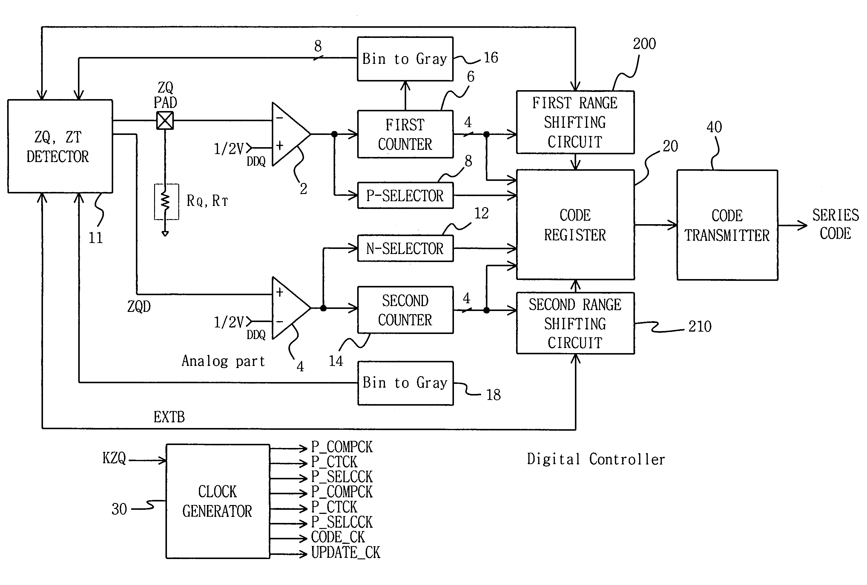
[0025]FIG. 4 is a block diagram of programmable impedance control circuit according to an exemplary embodiment of the invention. In comparing the circuit of FIG. 4 with a general programmable impedance control circuit of FIG. 3, first and second range shifting circuits 200 and 210 are additionally installed, each corresponding to back sides of first and second counter in the circuit of FIG. 4. An internal configuration of ZQ, ZT detector 11 shown in FIG....


PUM


Abstract

A programmable impedance control circuit for use in a semiconductor device having an impedance range shifting function prevents or substantially reduces an impedance detection failure based on an environment change. An impedance detector includes a first array driver, a second array driver, and an impedance matching transistor array and a range shifting transistor array independently controlled by the first and second array drivers. A comparator each compares first and second output voltage levels of the impedance detector with an array reference voltage, and outputs an up / down signal as the comparison result. A counter performs an up / down counting in response to the up / down signal, and outputs control code data. A range shifting circuit monitors a counting output of the counter and so generates range shifting data. Whereby, even if there is an environment change on a manufacturing process, power source voltage or operating temperature, etc., an impedance matching and correction operation can be performed without a waste of impedance matching transistor array and control code.

Description

CROSS REFERENCE TO RELATED APPLICATIONS[0001]This application claims priority from Korean Patent Application No. 2004-43416, filed on Jun. 14, 2004, the contents of which are hereby incorporated by reference for all purposes.BACKGROUND[0002]1. Field of the Invention[0003]The disclosure relates to an impedance control field of semiconductor device, and more particularly, to a programmable impedance control circuit for automatically correcting an impedance mismatching.[0004]2. Description of the Related Art[0005]Typically, semiconductor devices include input and output (I / O) pins for transmitting data from / to the outside world, and a data output circuit such as data output buffer and driver circuit, to provide internal data to the outside world. In integrating the semiconductor devices into electrical appliances, pins are connected to transmission lines such as a printed wiring, etc. on a mounting substrate. These pins are needed to charge and discharge a floating capacitance or load ...

Claims


Application Information

Patent Timeline
Patent Type & Authority Patents(United States)
IPC IPC(8): H03K17/16G11C5/00H03K19/0175H03K19/00
CPCH03K19/0005H03K19/0175
Inventor CHOI, MYUNG-HANLEE, YOUNG-DAEPARK, CHUL-SUNG
Owner SAMSUNG ELECTRONICS CO LTD
Why Eureka
Try Eureka