Crystallized glass spacer for field emission display and method its production

a technology of field emission display and crystallized glass, which is applied in the manufacture of glass tempering devices, electrode systems, electric discharge tubes/lamps, etc., can solve the problems of increasing the probability of cracking or chipping, reducing the yield, and high probability, and achieves low surface resistivity, high value of fracture toughness, and the effect of increasing the yield

Inactive Publication Date: 2008-04-29
ASAHI GLASS CO LTD
View PDF15 Cites 17 Cited by
  • Summary
  • Abstract
  • Description
  • Claims
  • Application Information

AI Technical Summary

Benefits of technology

[0017]It is an object of the present invention to provide a crystallized glass spacer with a high fracture toughness to prevent chipping or cracking of the spacer while keeping an appropriate electronic conductivity like glass spacers, a method for its production, and an FED using the above-mentioned crystallized glass spacer.
[0023]When the SiO2—TiO2-based glass is subjected to the reduction and crystallization heat treatment in the production method of the present invention, the crystallized glass spacer suitable for use in the FED is efficiently obtained with a low surface resistivity and a high value of fracture toughness. The spacer is unlikely to be charged and thus unlikely to cause distortion of the screen image, and provides a high-quality FED. Furthermore, the above-mentioned spacer contributes to increase of the yield because a probability of occurrence of a chip or a crack decreases in the assembly step of FED panels and other steps.

Problems solved by technology

When the glass spacers described above were used, there was, however, a problem that the glass spacers cracked or chipped in part because of their low fracture toughness during handling the glass spacers and bonding the glass spacers to a panel in a panel assembling step of FED, thereby decreasing the yield.
Furthermore, as the spacers become thinner for higher definition of FED as described above, it is highly likely that the probability of cracking or chipping will increase.

Method used


Image

  • Crystallized glass spacer for field emission display and method its production
  • Crystallized glass spacer for field emission display and method its production

Examples


example 1

Example of the Present Invention

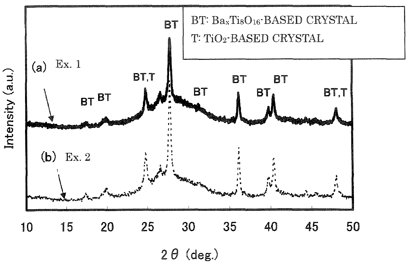
[0071]Raw materials were mixed in a composition of SiO2: 31 mol %, TiO2: 37 mol %, Al2O3: 3 mol %, CaO: 14 mol % and BaO: 15 mol %, and melted in a platinum or platinum-rhodium crucible under stirring and at 1400° C. in an air in an electric furnace for five hours. Then the molten glass was poured out to be formed into a plate, and slowly cooled.

[0072]The plate obtained by the above method was polished and cut in a size of 2×0.2×50 mm and in a shape of the spacer for the FED. Furthermore, a part of a small piece was cut into a predetermined size and polished to obtain test pieces. These processed products were introduced into a quartz tubular furnace and maintained at 740° C. for two hours under flow of hydrogen at a flow rate of 0.2 liter / min and nitrogen at a flow rate of 1.8 liters / min, and then the temperature was raised at a rate of 50° C. / hr up to 790° C. and maintained for 14 hours, whereby the reduction and crystallization heat treatment was c...

example 2

Example of the Present Invention

[0075]Raw materials were mixed in a composition of SiO2: 31 mol %, TiO2: 37 mol %, Al2O3: 3 mol %, CaO: 14 mol %, and BaO: 15 mol %, and melted in a platinum or platinum-rhodium crucible under stirring and at 1400° C. in an air in an electric furnace for five hours. Then the molten glass was poured out to be formed into a plate, and slowly cooled.

[0076]The plate obtained by the above method was polished and cut in a size of 2×0.2×50 mm and in a shape of the spacer for the FED. Furthermore, a part of a small piece was cut into a predetermined size and polished to obtain test pieces. These processed products were introduced into a quartz tubular furnace and maintained at 740° C. for two hours under flow of hydrogen at a flow rate of 1.4 liters / min and nitrogen at a flow rate of 0.6 liter / min, and then the temperature was raised at a rate of 50° C. / hr up to 810° C. and maintained for 6 hours, whereby the reduction and crystallization heat treatment was c...

example 3

Comparative Example

[0079]Raw materials were mixed in a composition of SiO2: 31 mol %, TiO2: 37 mol %, Al2O3: 3 mol %, CaO: 14 mol %, and BaO: 15 mol %, and melted in a platinum or platinum-rhodium crucible under stirring and at 1400° C. in an air in an electric furnace for five hours. Then the molten glass was poured out to be formed into a plate, and slowly cooled.

[0080]The plate obtained by the above method was polished and cut in a size of 2×0.2×50 mm and in a shape of the spacer for the FED. Furthermore, a part of a small piece was cut into a predetermined size and polished to obtain test pieces. However, no heat treatment was carried out for these processed products.

[0081]The value of fracture toughness KIC of the glass was measured and was as low as 0.62 MPa·m1 / 2, and a rate of occurrence of a chip or a crack was expected to be high when the glass was used for the spacer for the FED. Furthermore, the surface resistivity at 20° C. was 1016.2 Ω and no spacer obtained had a desir...


PUM

PropertyMeasurementUnit
temperatureaaaaaaaaaa
sizeaaaaaaaaaa
sizeaaaaaaaaaa

Abstract

Provided is a crystallized glass spacer for a field emission display resistant to charging with application of an electric field and resistant to chipping or cracking thanks to high fracture toughness.An SiO2—TiO2-based glass is subjected to a reduction and crystallization heat treatment at 600-900° C. in a hydrogen atmosphere or in a mixed atmosphere of hydrogen and nitrogen, to obtain a crystallized glass spacer for FED consisting essentially of, in molar percentage, SiO2: 20-50%, TiO2: 25-45%, MgO+CaO+SrO+BaO+ZnO: 20-50%, B2O3+Al2O3: 0-10% and ZrO2: 0-10%, and containing as a principal crystal at least one crystal selected from BaXTi8O16-based crystals (X=0.8-1.5), Ba2TiSi2O8-based crystals and TiO2-based crystals.

Description

BACKGROUND OF THE INVENTION[0001]1. Field of the Invention[0002]The present invention relates to a crystallized glass spacer with a high resistance to progress of destruction, i.e., a high fracture toughness and with an appropriate surface resistivity, a method for its production, and a field emission display (field emission-type display, which will be referred to hereinafter as “FED”).[0003]2. Discussion of Background[0004]An FED is an image display apparatus in which a large number of microscopic electron guns (cold-cathode elements) are arranged for each of pixels, and in which electron beams are emitted from the electron guns toward phosphors to form an image, like a cathode ray tube (Cathode Ray Tube, which will be referred to hereinafter as “CRT”).[0005]Since the FED arranged to independently drive the electron guns in each of the pixels, requires no scanning with an electron beam over a wide angle range unlike the CRT, an image display panel thereof can be made thinner and fl...

Claims


Application Information

Patent Timeline
Patent Type & Authority Patents(United States)
IPC IPC(8): C03C10/02C03C10/04
CPCC03B32/02C03C8/24C03C10/0009C03C10/0036H01J9/185H01J29/028H01J29/864H01J2329/864Y02P40/57
Inventor MIYAZAKI, SEIJIMAEDA, KEI
Owner ASAHI GLASS CO LTD
Why Eureka
Try Eureka