FET amplifier, pulse modulation module, and radar device

a pulse modulation module and amplifier technology, applied in gated amplifiers, using reradiation, instruments, etc., can solve the problems of gate bias voltage instability, inability to output inability to achieve a millimeter wave signal having a sufficient amplitude from the fet, etc., to achieve high output

Inactive Publication Date: 2008-04-29
MURATA MFG CO LTD
View PDF22 Cites 0 Cited by
  • Summary
  • Abstract
  • Description
  • Claims
  • Application Information

AI Technical Summary

Benefits of technology

[0014]In this unique construction, when a positive DC constant voltage and a fixed state signal voltage corresponding to the gate bias control signal in the Low state are input to the inverting amplifier, a positive gate bias voltage is generated to turn on the FET. Here, since a positive DC constant voltage input to the non-inverting input portion is input from a constant-voltage power supply, the voltage is stabilized, and, since a fixed voltage corresponding to the gate bias control signal input to the inverting input portion is 0 V in the Low state, the voltage in not affected by variation of the power supply voltage and is stable, and, as a result, the gate bias voltage output from the inverting amplifier is stable. Accordingly, the stable operation of the FET in the On state can be obtained.
[0017]In this unique construction, since the FET amplifier is stable and is ON / OFF operated at high speed, the amplitude of a high-frequency signal input to the FET can be stably ON / OFF controlled in a pulse shape and a pulse modulation signal having no dull waveform and no distortion can be output.
[0019]In this unique construction, when the pulse modulation module is used, the waveform as a pulse modulation signal does not become dull and is not distorted.

Problems solved by technology

However, in the related amplifiers, since the gate bias voltage of the FET is always negative, it is not able to output a millimeter wave signal having a sufficient amplitude from the FET.
However, in the related amplifiers, since the fixed gate bias voltage for making the FET in the ON state (making the FET have a large output amplitude) is generated by using the output voltage of a D / A converter, the gate bias voltage becomes unstable by the effect of variation of the power supply voltage of the D / A converter.
Thus, the amplitude of a millimeter wave signal output from the FET also becomes unstable.
Furthermore, as in Japanese Unexamined Patent Application Publication No. 11-195935, when a gate bias voltage is obtained by dividing a voltage by resistors, since the capacitance (capacitor) connected in parallel to the gate bias circuit and the resistors for voltage division constitute an integration circuit, a sharp waveform necessary for a high-speed pulse modulation cannot be obtained.

Method used


Image

  • FET amplifier, pulse modulation module, and radar device
  • FET amplifier, pulse modulation module, and radar device

Examples


Embodiment Construction

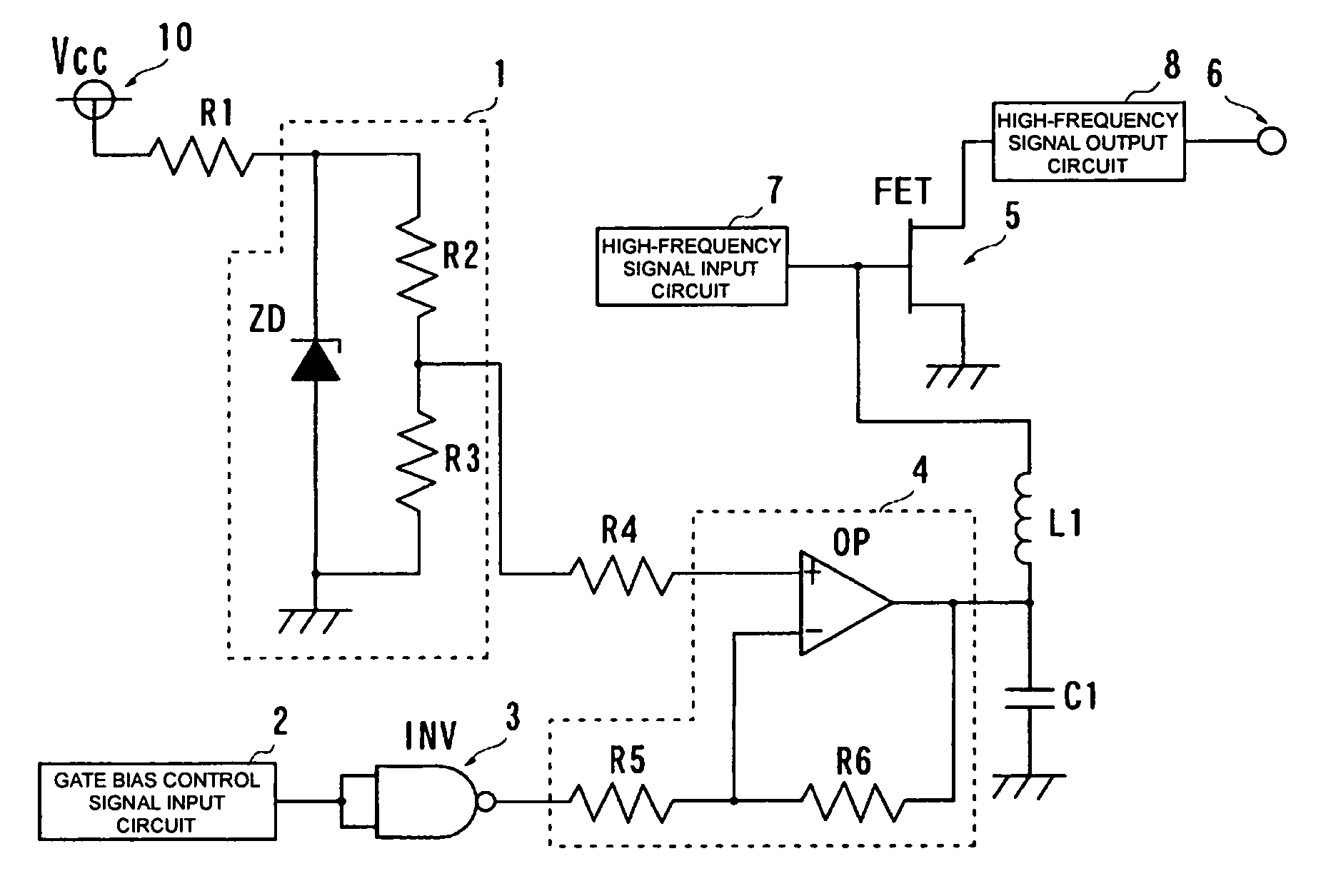
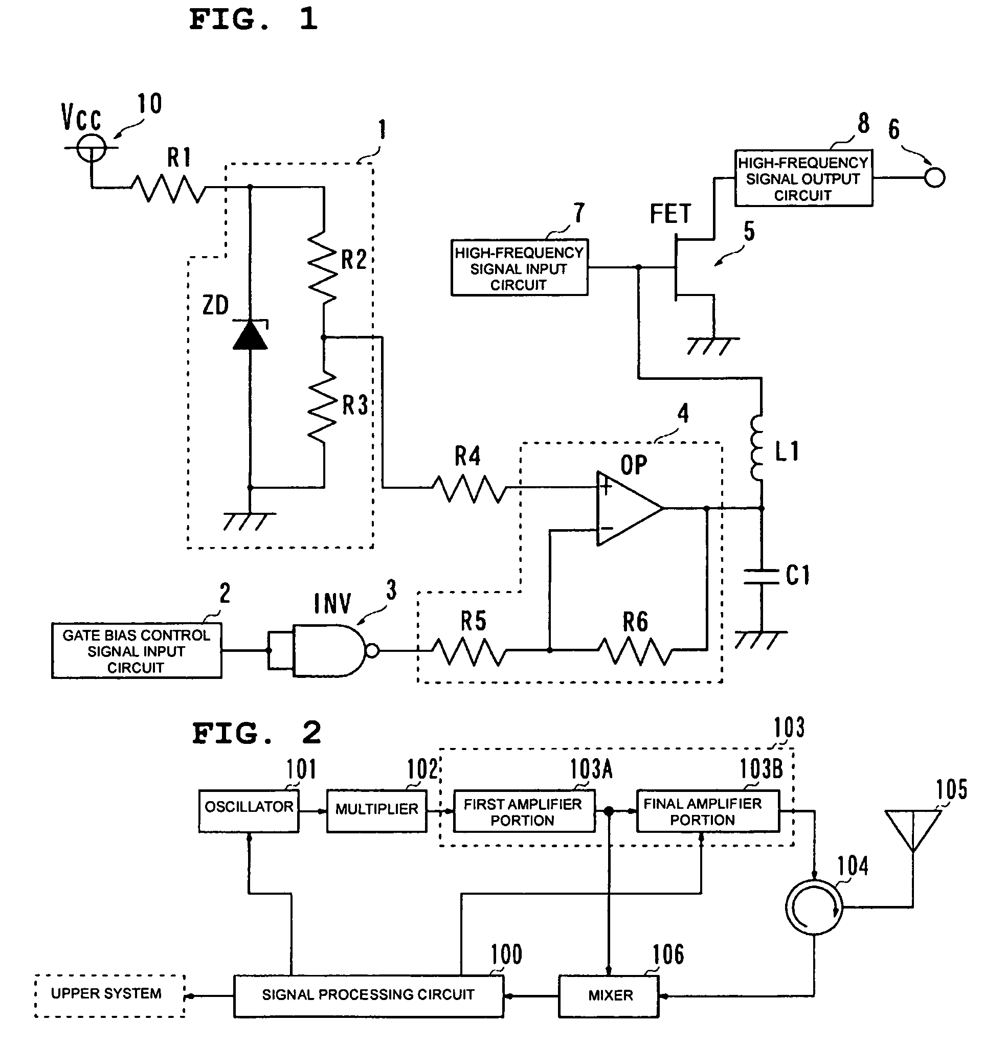
[0027]A pulse modulation module including an FET amplifier according to a first preferred embodiment of the present invention is described with reference to FIG. 1.

[0028]FIG. 1 is the circuit diagram of a pulse modulation module according to the present preferred embodiment.

[0029]As shown in FIG. 1, the gate of a depletion-type FET 5 in the pulse modulation module is made conductive to a high-frequency signal input circuit 7 and to the output portion of an inverting amplifier through an inductor L1. Furthermore, the source of the FET 5 is grounded and the drain is made conductive to a module signal output terminal 6 through a high-frequency signal output circuit 8.

[0030]The inverting amplifier 4 preferably includes an operational amplifier (differential amplifier) OP, a resistance element R6 connected between the inverting input terminal and the output terminal, and a resistance element R5 connected between the connection point of the inverting input terminal and the resistance elem...


PUM


Abstract

An FET amplifier includes an FET for amplifying a high-frequency signal to be input to the gate on the basis of a gate bias voltage from a gate bias control circuit. In the FET amplifier, a high-frequency signal input circuit and the output portion of an inverting amplifier are made conductive to the gate of the FET. A voltage stabilizing circuit generating a positive DC constant-voltage signal is made conductive to the non-inverting input portion of the inverting amplifier, and a gate bias control signal input circuit is made conductive to the inverting input portion through an inverter circuit. When the output voltage from the inverter circuit is 0 V, the inverting amplifier outputs a positive gate bias voltage (in the High state) and, when the output voltage from the inverter circuit is a fixed positive voltage, the inverting amplifier outputs a negative gate bias voltage (in the Low state) lower than the pinch-off voltage of the FET. The FET is ON / OFF controlled by the gate bias voltage and pulse modulates the input high-frequency signal to output the signal.

Description

BACKGROUND OF THE INVENTION[0001]1. Field of the Invention[0002]The present invention relates to an FET amplifier for amplifying a high-frequency signal, particularly an FET amplifier controlled by a gate bias control signal, a pulse modulation module for pulse modulating a high-frequency signal by using the FET amplifier, and a radar device for detecting a target by transmitting a pulse modulation signal from the pulse modulation module to the outside.[0003]2. Description of the Related Art[0004]As a device for detecting the distance to a target of a second vehicle existing in front of a first vehicle, etc., and the speed of the target, various millimeter wave radar devices are utilized and, among them, there are radar devices using an amplitude pulse modulation system. In a millimeter wave radar device using an amplitude pulse modulation system, a pulse modulation signal is generated and radiated by changing the amplitude of a high-frequency signal of a fixed frequency by an ON / OF...

Claims


Application Information

Patent Timeline
Patent Type & Authority Patents(United States)
IPC IPC(8): H03F3/04G01S7/28G01S7/282H03F1/30H03F3/189H03F3/72
CPCG01S7/282H03F1/301H03F3/72H03C1/62H03F1/30H03F3/193H03F3/21H03F3/189
Inventor YAMASHITA, SADAO
Owner MURATA MFG CO LTD
Why Eureka
Try Eureka