Substrate processing apparatus and substrate processing method

a substrate processing and substrate technology, applied in the field of substrate processing, can solve the problems of difficult depositing, complicated processing and maintenance of the gas diffusion plate 108, and further reduction of the size of the elements in the semiconductor integrated circuit devi

Active Publication Date: 2008-05-06
PANNOVA SEMIC
View PDF15 Cites 4 Cited by
  • Summary
  • Abstract
  • Description
  • Claims
  • Application Information

AI Technical Summary

Benefits of technology

[0021]It is preferable that a difference between respective areas of the inlet and outlet of one of the plurality of through holes provided in the peripheral region of the gas diffusion plate is larger at a greater distance from the center region of the gas diffusion plate. Thus, ones of the through holes provided at a greater distance from the center region of the gas diffusion plate can take in a larger amount of a processing gas. As a result, a difference in the density of a process gas in part of the shower head over the gas diffusion plate can be corrected and thus a substrate can be uniformly processed. Specifically, when the through holes are formed using a drill, uniform substrate processing can be performed with high accuracy by adjusting a difference in area between the inlet and outlet thereof.
[0042]Moreover, in one embodiment of the present invention, each one of the through holes provided in the peripheral region of the gas diffusion plate comprises an inlet-side portion including the inlet and an outlet-side portion including the outlet, each of the inlet- and outlet-side portions is formed in a pillar shape so as to have a certain opening area, and a depth of the inlet-side portion is larger at a greater distance from the center region. Thus, in the step b), by adjusting the depth of the inlet-side portions, substrate processing can be uniformly performed with high accuracy.

Problems solved by technology

In such a case, however, processing and maintenance of the gas diffusion plate 108 would become complicated.
However, as the size of elements in the semiconductor integrated circuit devices is further reduced in future and more precise process control is required, it becomes difficult to deposit, using the shower head 102 in the known chemical vapor deposition apparatus of FIG. 6, a film with sufficiently high uniformity of film thickness for fabricating a semiconductor integrated circuit device with high yield.
However, to fabricate a fine semiconductor integrated circuit having a dimension of ¼μm or less, the above-described etching uniformity is not sufficient, and higher uniformity is required.
Moreover, it can be assumed that if the technique is used for a gas diffusion plate in a chemical vapor deposition apparatus, uniformity of flow rate distribution of a source gas can not reach a sufficiently high level for fabricating a semiconductor integrated circuit.
That is, according to the known method, uniformity sensitively varies with respect to adjustment of the through holes and the distribution of the through holes and therefore it is very difficult to achieve uniformity of 3% on an average or higher uniformity.

Method used


Image

  • Substrate processing apparatus and substrate processing method
  • Substrate processing apparatus and substrate processing method
  • Substrate processing apparatus and substrate processing method

Examples


first embodiment

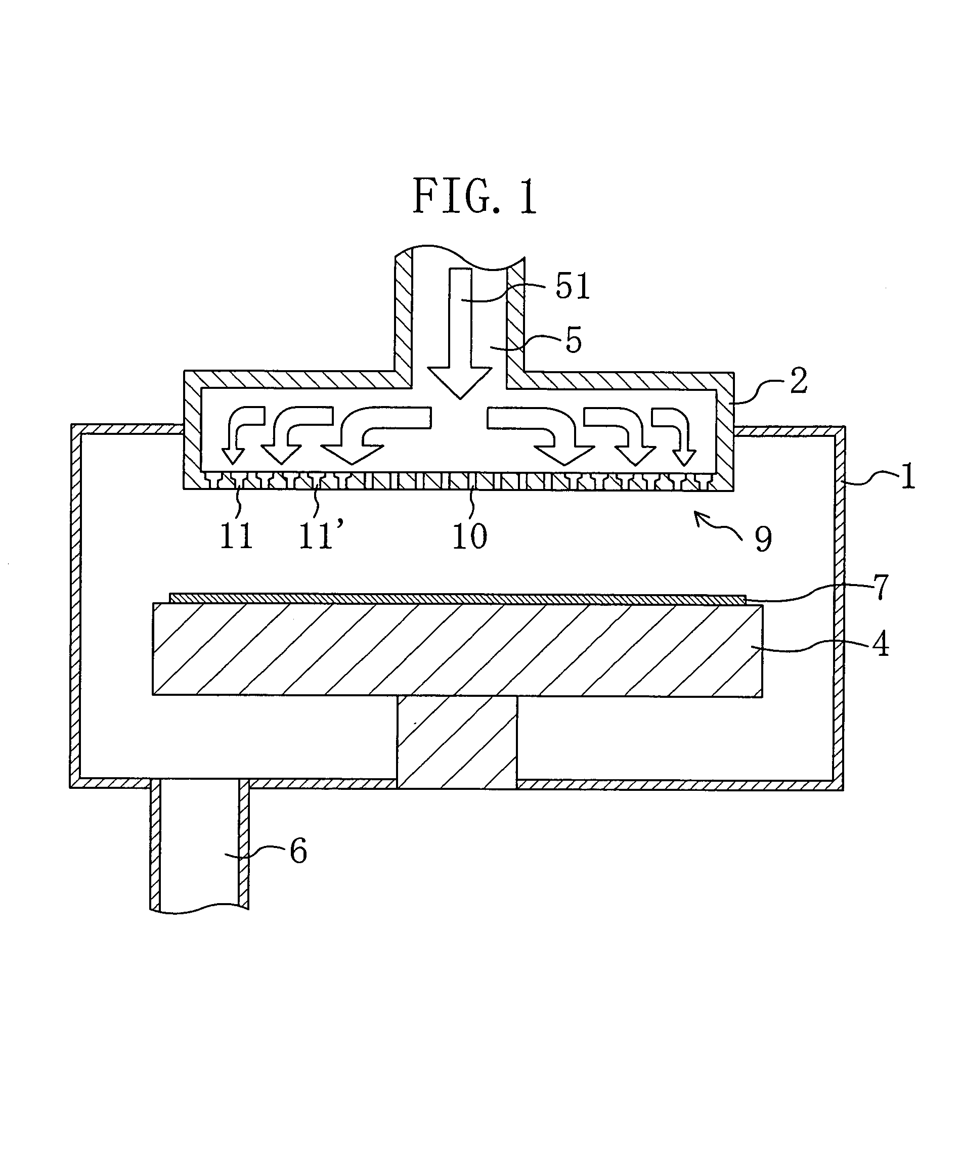
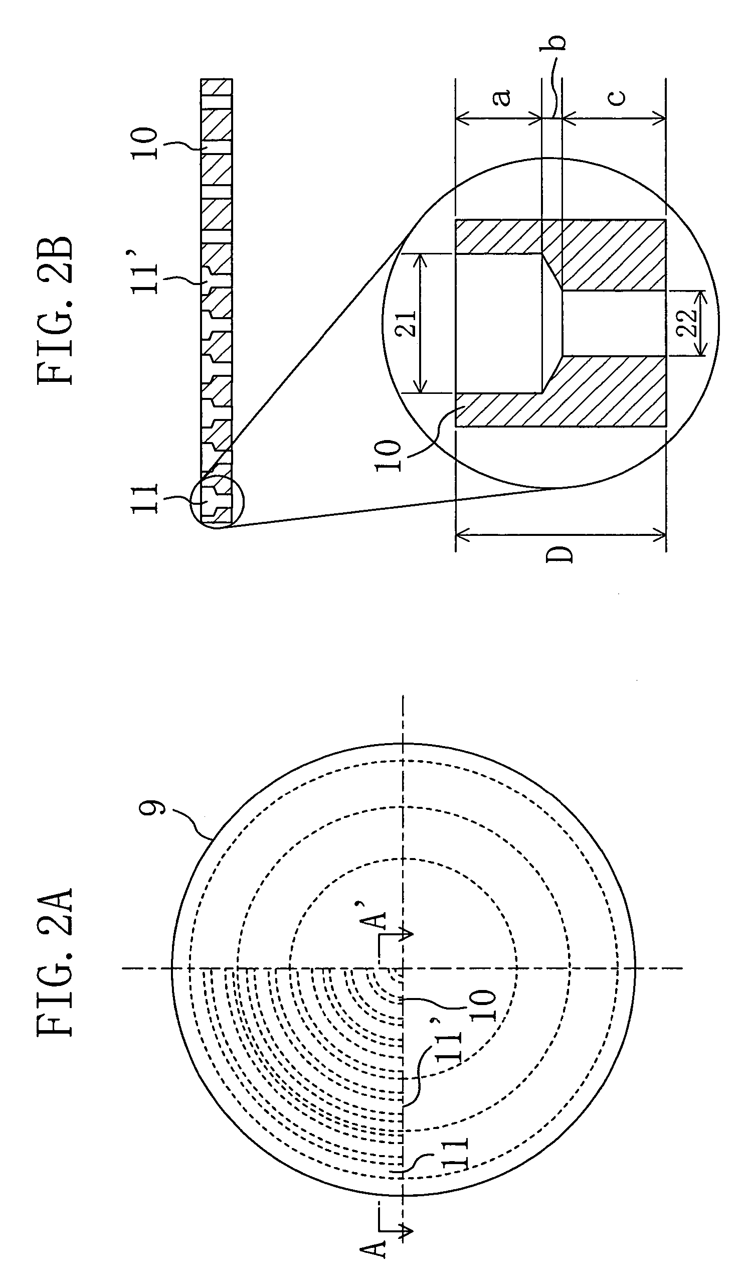
[0051]FIG. 1 is a cross-sectional view illustrating the inner structure of a chemical vapor deposition apparatus (substrate processing apparatus) according to a first embodiment of the present invention for use in fabricating a semiconductor integrated circuit. As shown in FIG. 1, the chemical vapor deposition apparatus includes a gas diffusion plate in which through holes are formed so as to have a different shape, compared to the known chemical vapor deposition apparatus of FIG. 6.

[0052]Specifically, the chemical vapor deposition apparatus of this embodiment includes a reaction chamber 1 for forming a thin film on a semiconductor substrate (substrate) 7 using a source gas (processing gas) 51, a shower head 2 for supplying the source gas 51 to the inside of the reaction chamber 1, to which a gas diffusion plate 9 is attached and in which a plurality of through holes for flowing the source gas 51 are formed and which has a plate shape, and a substrate support 4, provided in the reac...

second embodiment

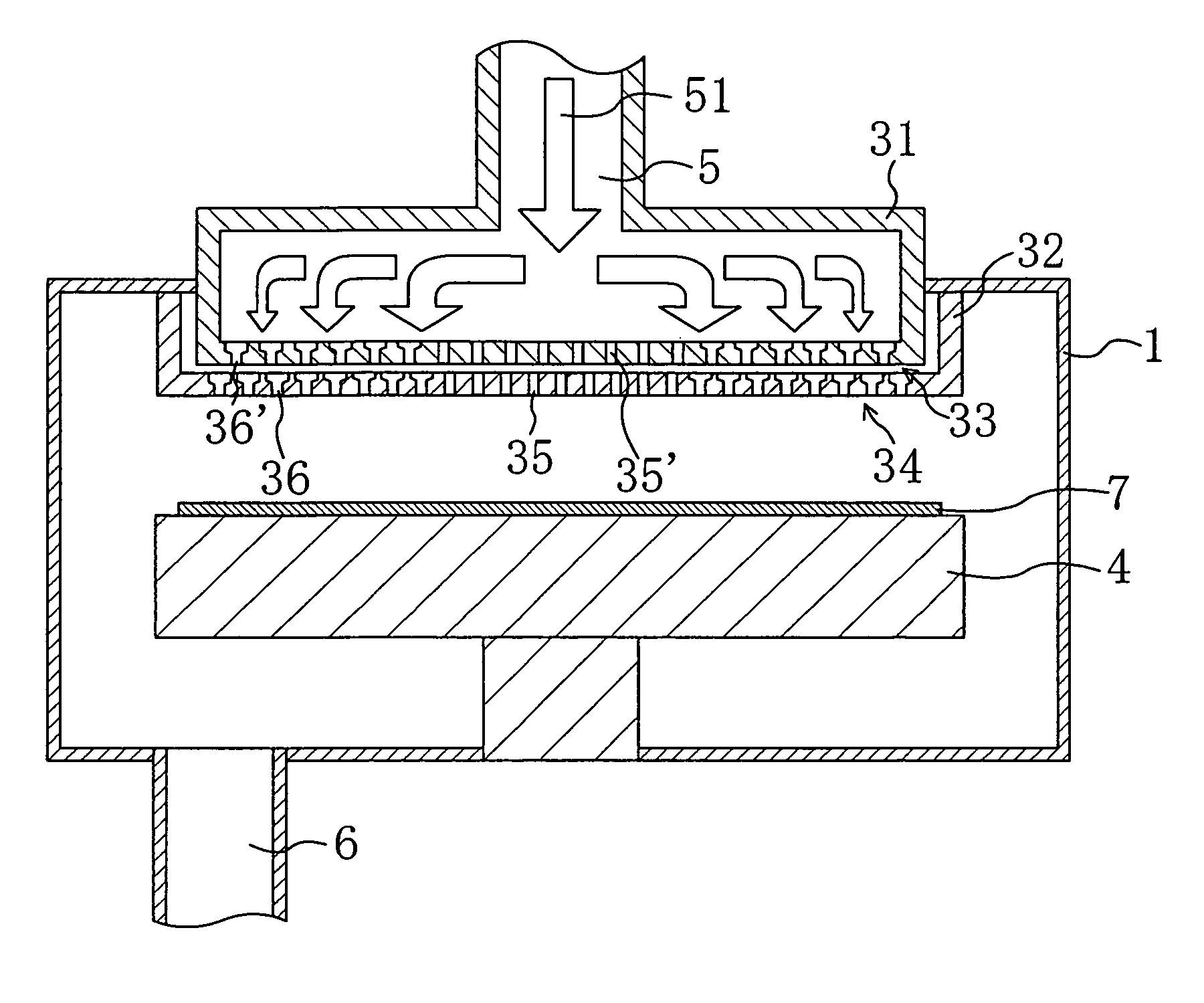
[0072]FIG. 4 is a cross-sectional view illustrating the internal structure of a chemical vapor deposition apparatus according to a second embodiment of the present invention. The structure of the chemical vapor deposition apparatus of this embodiment is generally the same as that of the chemical vapor deposition apparatus of the first embodiment, but shower heads 2 for discharging a source gas serving as a film formation material are doubly provided. The gas diffusion plate of the first embodiment is used for each of the shower heads 2. The chemical vapor deposition apparatus of this embodiment is characterized by this double shower head structure. In FIG. 4, each member of the chemical vapor deposition apparatus also shown in FIG. 1 is identified by the same reference numeral and therefore the description thereof will be omitted.

[0073]As shown in FIG. 4, in the chemical vapor deposition of this embodiment, a first shower head to which a first gas diffusion plate 33 is attached has ...


PUM

PropertyMeasurementUnit
diameteraaaaaaaaaa
thicknessaaaaaaaaaa
diameteraaaaaaaaaa

Abstract

A substrate processing apparatus includes a reaction chamber with a structure allowing pressure reduction, a shower head for supplying a processing gas into the reaction chamber including a gas diffusion plate in which through holes are formed, and a substrate support for placing a substrate. Each ones of through holes provided in a peripheral region of the gas diffusion plate is formed so that an area of an inlet thereof is larger than an area of an outlet thereof. With use of the substrate processing apparatus, a processing gas can be supplied uniformly in the gas diffusion plate. Therefore, substrate processing such as film deposition and film etching can be uniformly performed.

Description

CROSS-REFERENCE TO RELATED APPLICATION[0001]This application claims priority under 35 U.S.C. §119(a) on Japanese Patent Application No. 2004-307060 filed on Oct. 21, 2004, the entire contents of which are hereby incorporated by reference.BACKGROUND OF THE INVENTION[0002]1. Field of the Invention[0003]The present invention relates to substrate processing such as film formation performed using a chemical vapor deposition apparatus and fine processing performed using a dry etching apparatus, and more particularly relates to a technique for improving uniformity of processing.[0004]2. Prior Art[0005]In recent years, there has been a trend where the degree of integration of semiconductor integrated circuit devices is further increased whereas the power consumption thereof is further reduced. Meanwhile, costs in semiconductor integrated circuit device fabrication have been reduced by increase in the diameter of semiconductor substrates and the like. In order to reduce pattern dimensions of...

Claims


Application Information

Patent Timeline
Patent Type & Authority Patents(United States)
IPC IPC(8): H01L21/31
CPCC23C16/45565
Inventor MATSUBARA, TOSHIOSATOH, HIROYUKIUCHIJIMA, HIDETO
Owner PANNOVA SEMIC
Why Eureka
Try Eureka