Image sensor and method for fabricating the same

a technology of image sensor and manufacturing method, which is applied in the direction of diodes, basic electric elements, electric apparatus, etc., can solve the problems of high fabrication cost, difficulty in improving electric contact quality, and the trend of decreasing use of ccd, so as to improve contact quality and improve contact quality

Inactive Publication Date: 2008-05-20
COLUMBA TECH INC
View PDF18 Cites 1 Cited by
  • Summary
  • Abstract
  • Description
  • Claims
  • Application Information

AI Technical Summary

Benefits of technology

[0018]An object of the present invention is to provide an image sensor and a method for fabricating the same, in which an impurity implantation layer of a constant thickness, having an impurity selectively implanted thereto, is additionally formed on a source diffusion layer, to control a substantial contact point between a contact plug and the source diffusion layer upward from a surface of a semiconductor substrate, so that it is possible to realize an open hole of a sufficient size by minimizing a length of the open hole which is a main channel of the contact plug, thereby improving a contact quality between the contact plug and the source diffusion layer.
[0019]Another object of the present invention is to provide an image sensor and a method for fabricating the same, to realize a high-impurity concentration in a source diffusion layer without troubles generated by high impurity implantation of the source diffusion layer and by formation of a salicide layer, thereby improving a contact quality between a contact plug and the source diffusion layer.

Problems solved by technology

However, the CCD has the disadvantageous characteristics of requirements for a high driving voltage and an additional supporting circuit, and of a high fabrication cost, whereby the CCD is a decreasing trend in use.
However, the related art CMOS image sensor has difficulties in improving the electric contact quality between the contact plug 24 and the source diffusion layer 16.
Thus, it has the limitation to the increase in amount of impurity implanted to the source diffusion layer 16, thereby causing the deterioration of the electric contact quality between the contact plug 24 and the source diffusion layer 16.

Method used


Image

  • Image sensor and method for fabricating the same
  • Image sensor and method for fabricating the same
  • Image sensor and method for fabricating the same

Examples


Embodiment Construction

[0028]Reference will now be made in detail to the preferred embodiments of the present invention, examples of which are illustrated in the accompanying drawings. Wherever possible, the same reference numbers will be used throughout the drawings to refer to the same or like parts.

[0029]Hereinafter, an image sensor and a method for fabricating the same according to the present invention will be described with reference to the accompanying drawings.

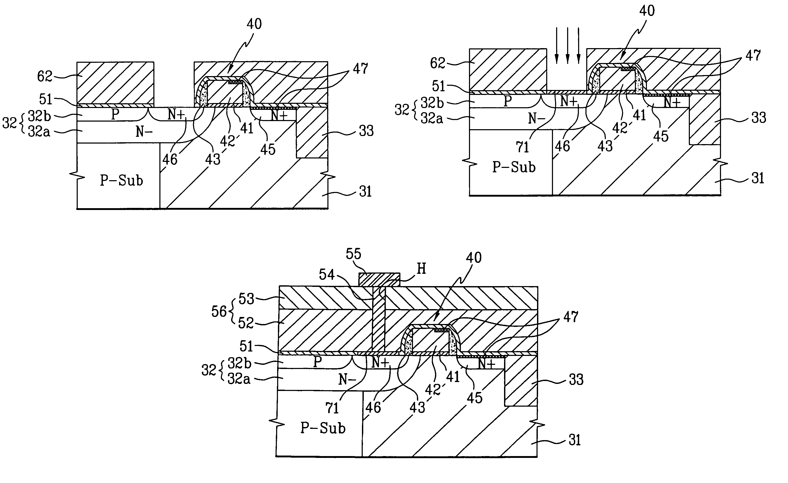
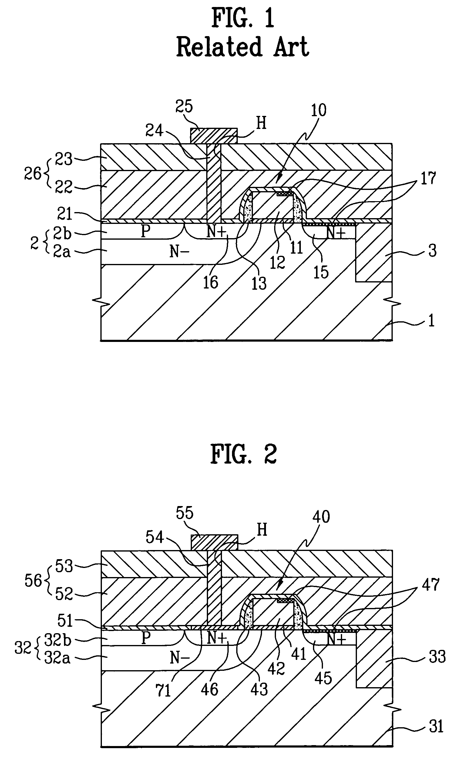
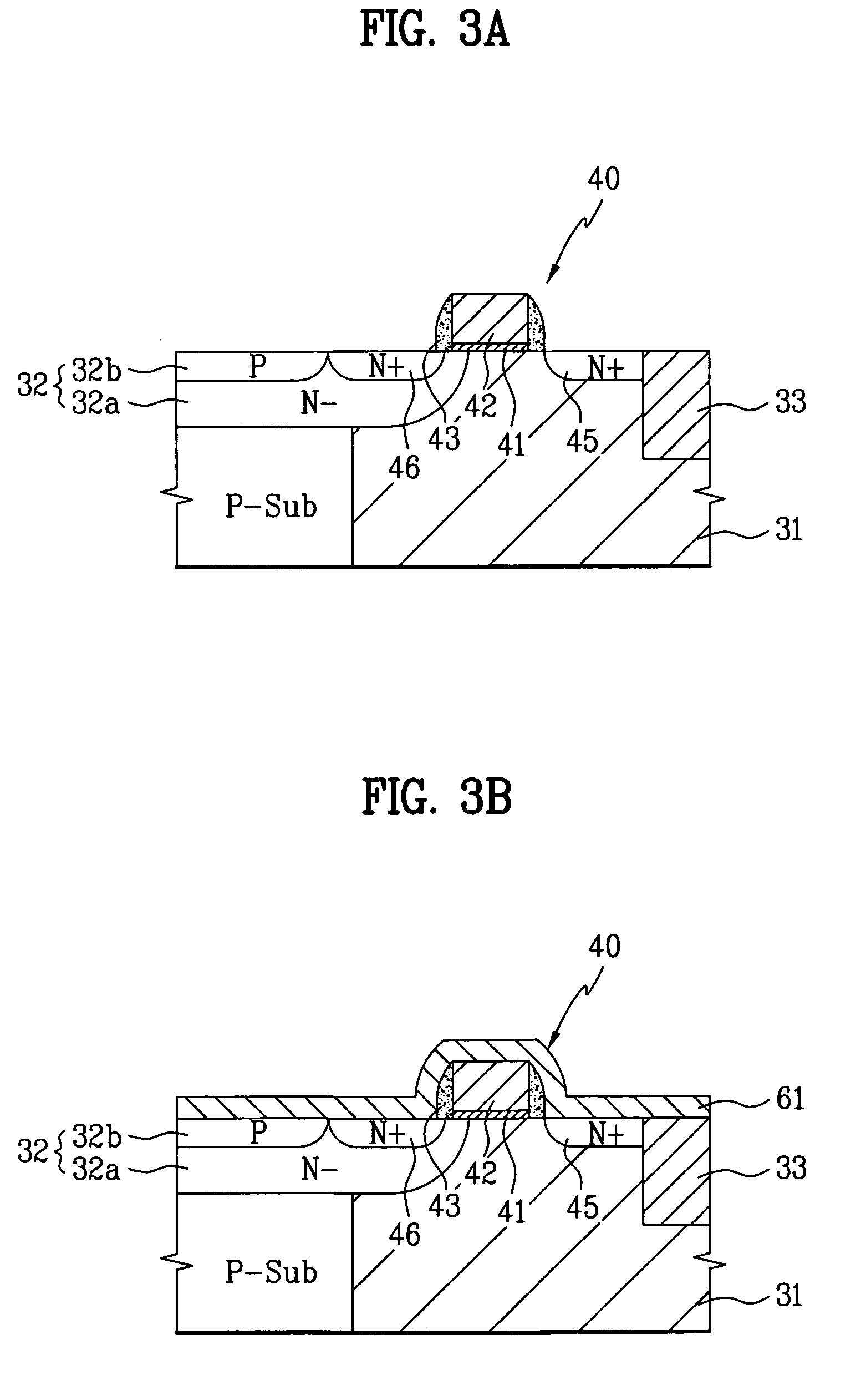
[0030]As shown in FIG. 2, a CMOS image sensor according to the present invention is formed in an active area of a semiconductor substrate 31 defined by a device isolation layer 33, wherein the CMOS image sensor is comprised of a photodiode 32 for receiving the incident light from the external and generating optical charges, and a transistor 40 for transferring / discharging the optical charges generated in the photodiode 32 to a signal processing circuit.

[0031]For example, the photodiode 32 is comprised of a P-type impurity diffusion layer 32b...


PUM


Abstract

An image sensor and a method for fabricating the same are disclosed, to improve a contact quality between a contact plug and a source diffusion layer. The image sensor includes a photodiode in an active area of a semiconductor substrate, for receiving incident external light and generating optical charges; a transistor having an impurity diffusion layer electrically connected with the photodiode, for transferring / discharging the optical charges generated by the photodiode to a signal processing circuit; an impurity implantation layer having impurity selectively implanted thereto, for selectively covering the impurity diffusion layer; an insulating interlayer above the semiconductor substrate to cover the photodiode, the transistor, and the impurity implantation layer; an open hole penetrating the insulating interlayer, for selectively opening the impurity diffusion layer; and a contact plug for filling the open hole, and electrically connecting the impurity diffusion layer and a metal line provided above the insulating interlayer.

Description

[0001]This application claims the benefit of the Korean Application No. P2003-101698 filed on Dec. 31, 2003, which is hereby incorporated by reference.BACKGROUND OF THE INVENTION[0002]1. Field of the Invention[0003]The present invention relates to an image sensor, and more particularly, to an image sensor and a method for fabricating the same, to improve a contact quality between a contact plug and a source diffusion layer by forming an impurity implantation layer, having an impurity selectively implanted thereto, on the source diffusion layer, thereby realizing an optimal image quality in the completed image sensor.[0004]2. Discussion of the Related Art[0005]In recent, as a rapid development of electrical and electronic technologies, various electronic equipments using an image sensor technology, for example, a video camera, a digital camera, a personal computer having a small-sized camera, a mobile phone having a small-sized camera, etc. have been widely studied and researched, an...

Claims


Application Information

Patent Timeline
Patent Type & Authority Patents(United States)
IPC IPC(8): H01L21/44H01L21/285H01L23/52H01L27/146H01L31/0232H01L31/10
CPCH01L21/28525H01L27/14609H01L27/14636H01L27/14643H01L27/14687H01L27/14689H01L21/76814H01L27/146H01L31/10
Inventor SHIM, HEE SUNG
Owner COLUMBA TECH INC
Why Eureka
Try Eureka