Method for providing layout design and photo mask

a technology of layout design and mask, applied in the field of providing layout design and photo mask, can solve the problems of increasing the size and area of the whole chip, and achieve the effect of reducing the entire area of the pattern

Inactive Publication Date: 2008-05-20
RENESAS ELECTRONICS CORP
View PDF7 Cites 183 Cited by
  • Summary
  • Abstract
  • Description
  • Claims
  • Application Information

AI Technical Summary

Benefits of technology

[0029]In the present invention, the arrangement of the hole patterns and the manufacture of the photo mask are conducted by either one of the above-described methods for providing the layout design. Thus, the area of the chip in the semiconductor integrated circuit manufactured by employing this photo mask can be smaller than the conventional chip. Therefore, the entire area of the pattern can be reduced, while maintaining the advantageous effect obtainable by disposing the hole patterns at the mesh points of the virtual grid.

Problems solved by technology

The increase of area of such primitive cell, in turn, leads to an increase of size and area of the whole chip.

Method used


Image

  • Method for providing layout design and photo mask
  • Method for providing layout design and photo mask
  • Method for providing layout design and photo mask

Examples


first embodiment

[0046]Configurations of the present invention will be described.

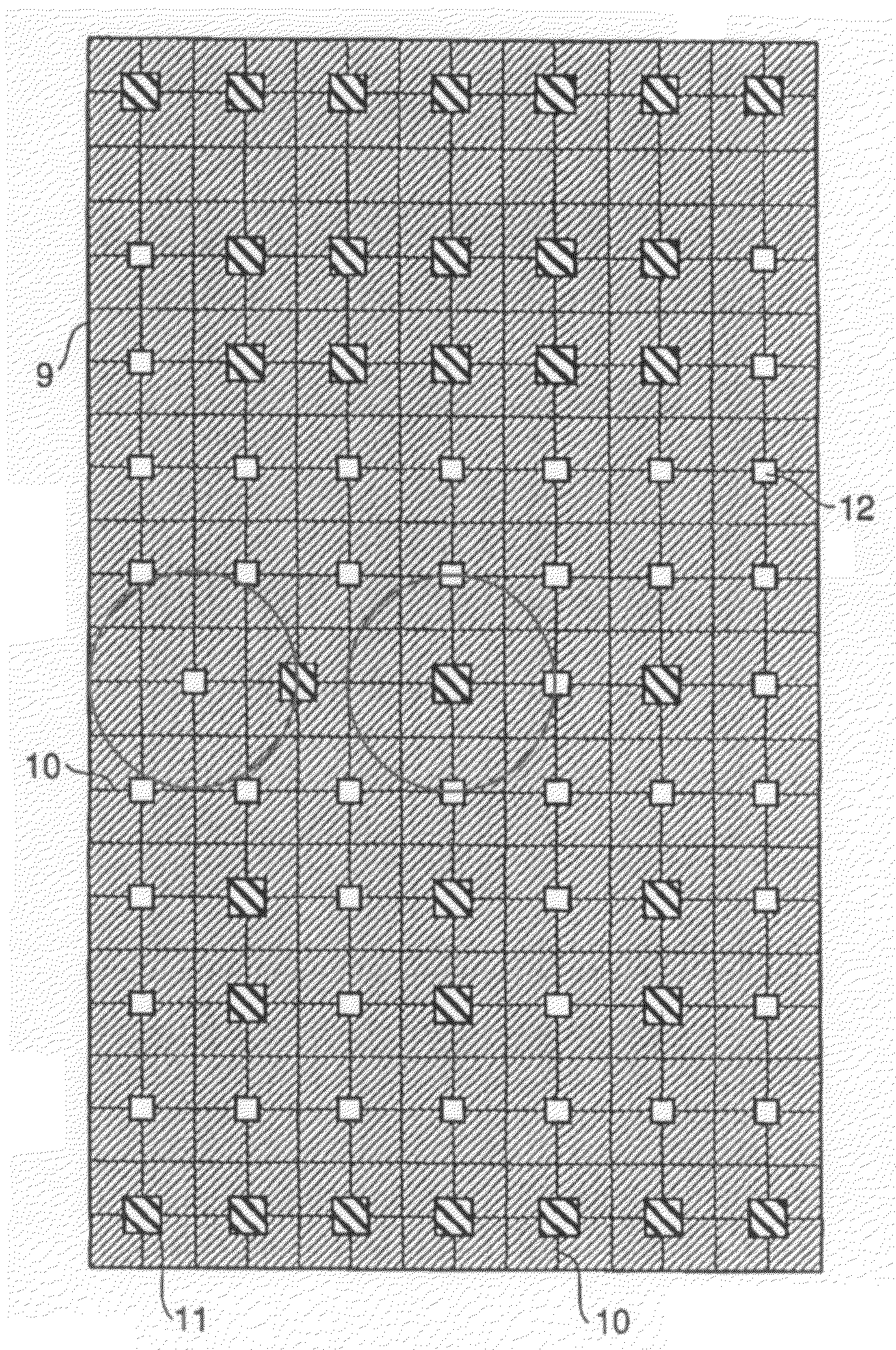
[0047]FIG. 1 is a schematic diagram, showing a layout pattern of an example of a primitive cell according to a method for providing layout design of the present invention. FIG. 1 shows a case of a dual-input NAND gate.

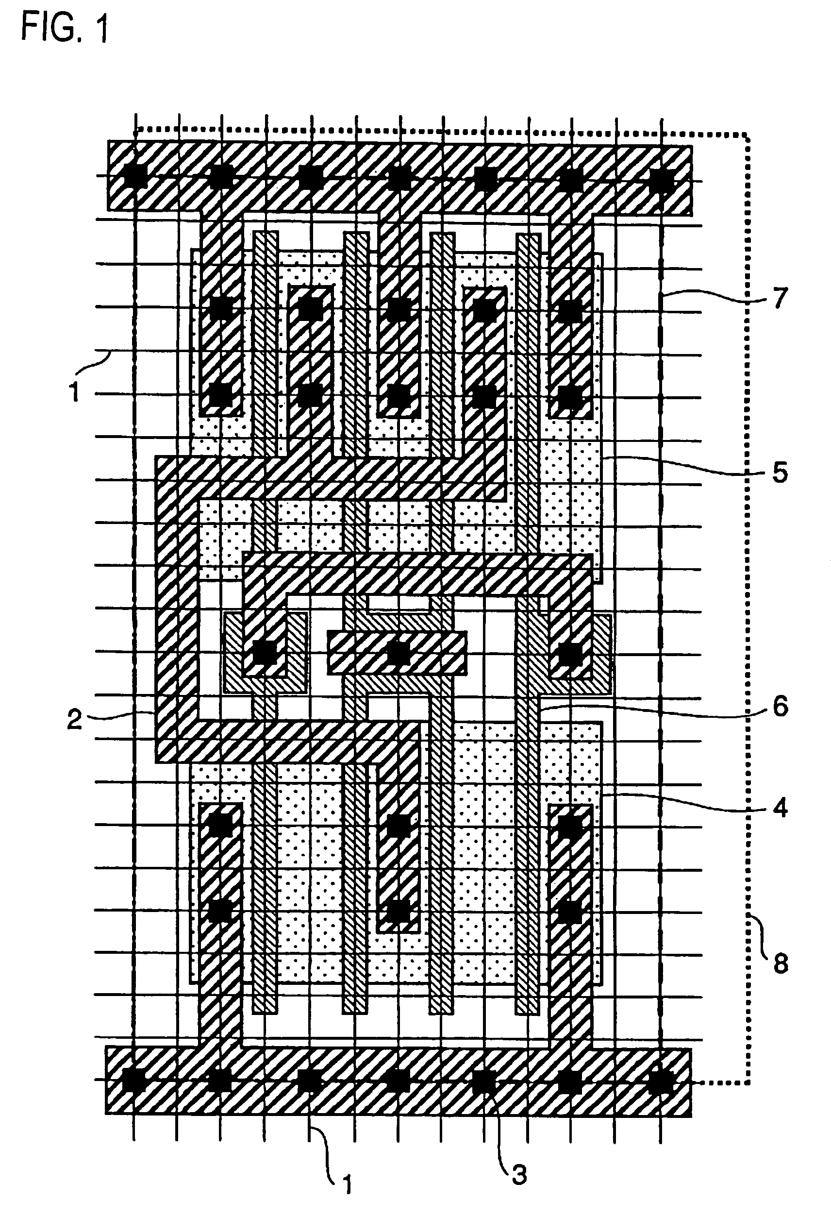
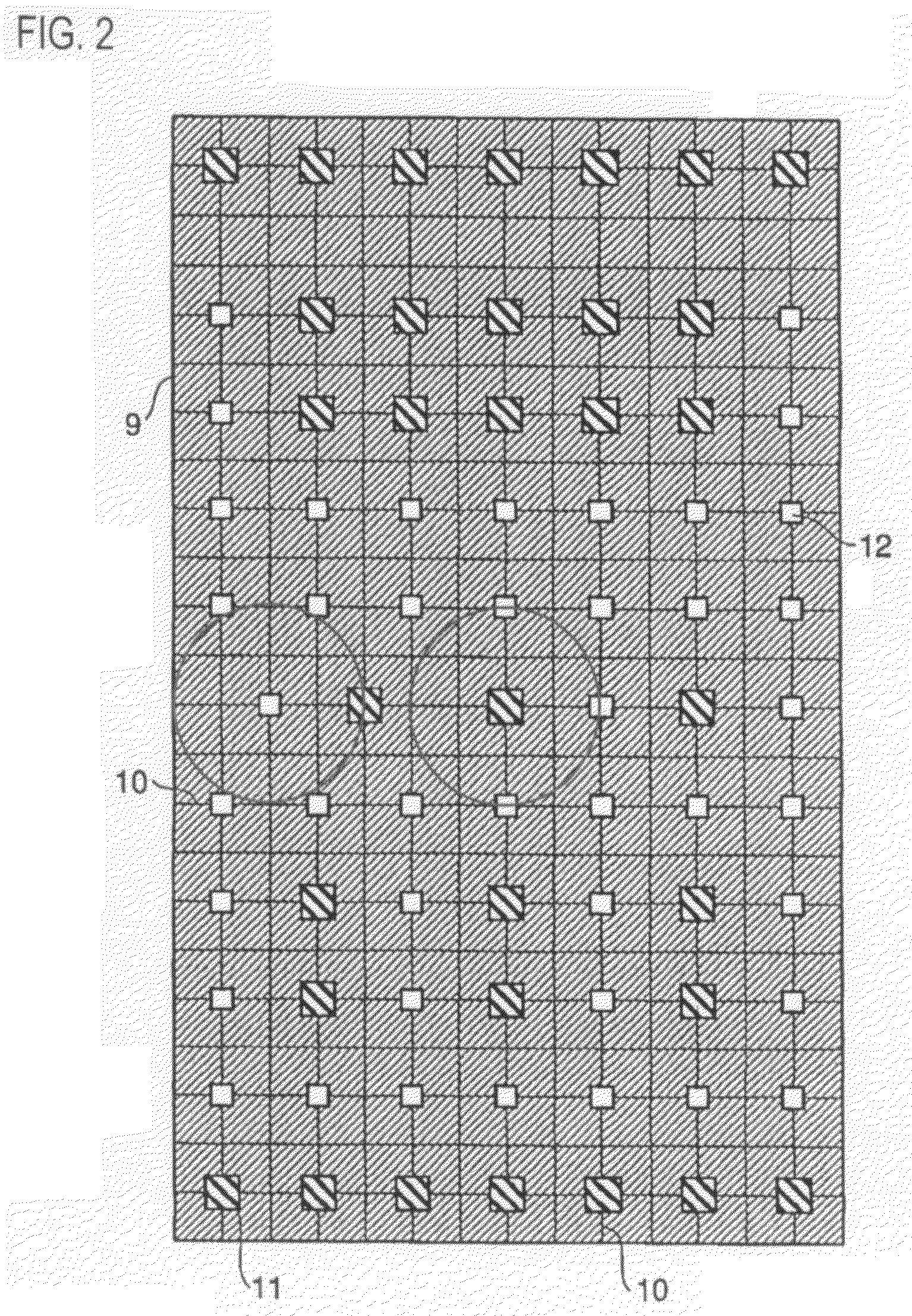
[0048]As shown in FIG. 1, similarly as in the conventional configuration, a primitive cell has a P-type transistor and a N-type transistor, and respective contact holes 3 are disposed on mesh points of a virtual grid 1 having mutually orthogonal lines.

[0049]In the present embodiment, a virtual grid size, which is defined as a mesh size of the virtual grid, is smaller than the resolution limit pitch for the contact holes 3. In addition, two folds of the virtual grid size is equal to or larger than the resolution limit pitch. While the contact holes are disposed at the mesh points of the virtual grid 1, when a specific hole of the hole patterns is considered, the most adjacent mesh point thereof is free of a...

second embodiment

[0065]The present embodiment is characterized in that the virtual grid size along the X direction of the transverse direction in the virtual grid shown in FIG. 1 in the first embodiment is different from that along the Y direction of a longitudinal direction.

[0066]Configuration of the present embodiment will be described. Similar numeral is assigned to a similar element appeared in the first embodiment, and the detailed description thereof is not presented.

[0067]FIG. 3 is schematic diagram, showing the layout pattern of a primitive cell obtained by a method for providing the layout design according to the present embodiment. FIG. 3 shows a case of the dual-input NAND gate, similarly as in the first embodiment.

[0068]X-direction virtual grid 31a in FIG. 3 comprises grid lines of X0 to X12 and Y-direction virtual grid 31b comprises grid lines of Y0˜Y15. The virtual grid size in X direction is smaller than the resolution limit pitch for the contact holes 11, similarly as in the first em...


PUM

PropertyMeasurementUnit
sizeaaaaaaaaaa
sizeaaaaaaaaaa
wave lengthaaaaaaaaaa

Abstract

A method for providing the layout design of semiconductor integrated circuit that is capable of promoting the reduction of the circuit pattern area is provided. A hole pattern is disposed at the mesh point which is an intersecting point of mutually orthogonal virtual grid lines and another hole pattern is not disposed at the adjacent mesh point that is the closed mesh point having the hole pattern thereon.

Description

[0001]The present application is based on Japanese patent application No. 2003-424914, the whole contents of which are herein incorporated by reference.BACKGROUND OF THE INVENTION[0002]1. Field of the Invention[0003]The present invention relates to a method for providing a layout design and a photo mask.[0004]2. Related Art[0005]Layout designs for providing patterns such as contact holes, interconnects or the like of a semiconductor integrated circuit depends upon types of circuits. In a large scale integrated circuit of the standard cell design having a plurality of predetermined logic circuits disposed thereon as unit circuits, a layout design technique of arranging hole patterns of contact holes, via holes and the like at mesh points of orthogonally intersecting virtual grid is employed. The reasons for disposing the hole patterns at the mesh points generally include two reasons.[0006]One reason is that the technique is suitable to be adopted for the automated interconnect layout...

Claims


Application Information

Patent Timeline
Patent Type & Authority Patents(United States)
IPC IPC(8): G06F17/50G03F1/00G03F1/36G03F1/70H01L21/027H01L21/82H01L27/02H01L27/118
CPCG03F1/144H01L27/0207H01L27/118G03F1/36G03F7/70433
Inventor KOKUBUN, TETSUYA
Owner RENESAS ELECTRONICS CORP
Why Eureka
Try Eureka