

Methods of fabricating a semiconductor device having a node contact structure of a CMOS inverter
a node contact structure and semiconductor technology, applied in the direction of semiconductor devices, electrical equipment, transistors, etc., can solve the problems of weak latch-up immunity, lower integration density of bulk cmos sram cells, and difficulty in converting body layers into perfect single crystalline silicon layers,
- Summary
- Abstract
- Description
- Claims
- Application Information
AI Technical Summary
Benefits of technology
Problems solved by technology
Method used
Image

Examples
Embodiment Construction
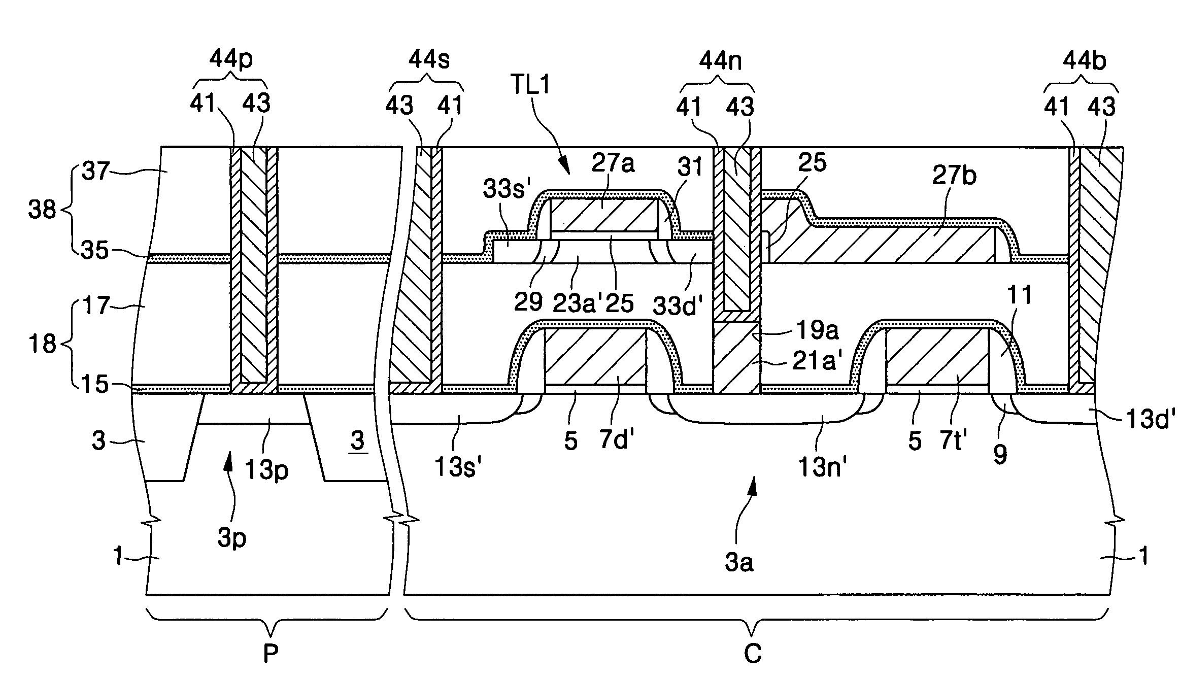
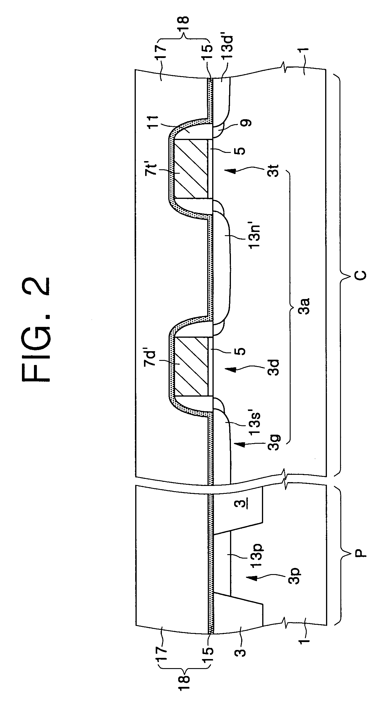
[0027]The present invention will now be described more fully with reference to the accompanying drawings, in which exemplary embodiments of the invention are shown. The invention may, however, be embodied in many different forms and should not be construed as being limited to the embodiments set forth herein. Rather, these embodiments are provided so that this disclosure will be thorough and complete, and will fully convey the concept of the invention to those skilled in the art. In the drawings, the thicknesses of layers and regions are exaggerated for clarity. Like reference numerals in the specification denote like elements.
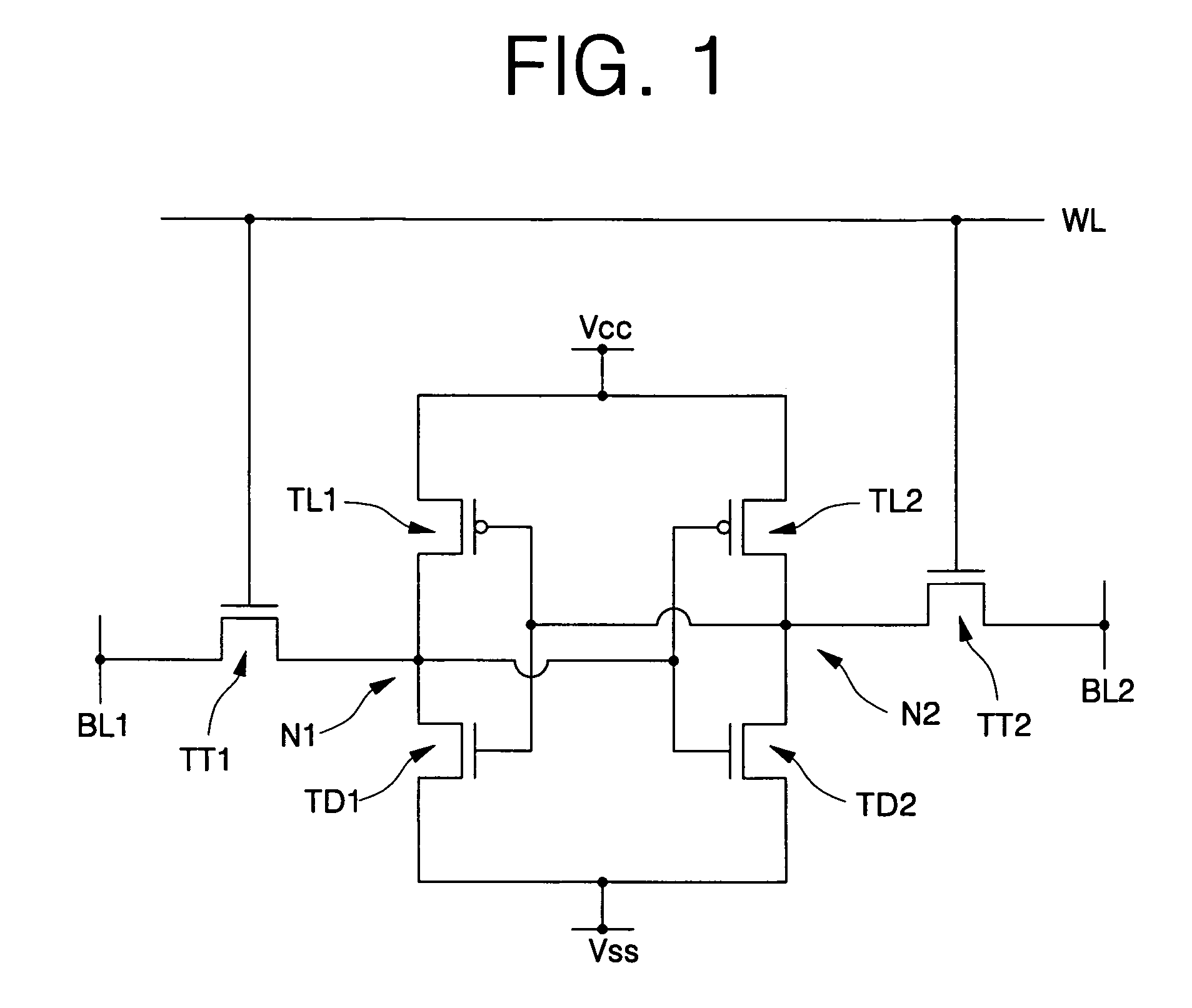
[0028]FIG. 1 is an equivalent circuit diagram of a CMOS SRAM cell, such as a TFT SRAM cell or a bulk CMOS SRAM cell.
[0029]Referring to FIG. 1, the CMOS SRAM cell comprises a pair of driver transistors TD1 and TD2, a pair of transfer transistors TT1 and TT2, and a pair of load transistors TL1 and TL2. The pair of driver transistors TD1 and TD2 and the pair of t...
PUM
 Abstract
Description
Claims
Application Information