High performance field effect transistors on SOI substrate with stress-inducing material as buried insulator and methods

a stress-inducing material and high-performance technology, applied in the direction of semiconductor devices, semiconductor/solid-state device details, electrical apparatus, etc., can solve the problems of device performance suffer, strain in the channel region decreases, device stress is strongly dependent on such fet devices, etc., and achieves performance enhancement

Inactive Publication Date: 2008-06-17
GLOBALFOUNDRIES INC
View PDF5 Cites 29 Cited by
  • Summary
  • Abstract
  • Description
  • Claims
  • Application Information

AI Technical Summary

Benefits of technology

[0008]Additionally, since the FETs of the present invention are located on a SOI substrate, those devices have several advantages over more conventional FET devices that are located on a bulk semiconductor. For example, SOI devices may have lower power consumption requirements than other types of devices that perform similar tasks. SOI devices may also have lower parasitic capacitances than non-SOI devices. This translates into faster switching times for the resulting circuits. In addition, the phenomenon of “latchup,” which is often exhibited by complementary metal oxide semiconductor (CMOS) devices, may be avoided when circuit devices are manufactured using SOI fabrication processes. SOI devices are also less susceptible to the adverse effects of ionizing radiation and, therefore, tend to be more reliable in applications where ionizing radiation may cause operation errors.
[0010]The inventive structure is particularly useful with ultra-thin semiconductor-on-insulator (UTSOI) devices since such devices will benefit the most from a stress-inducing insulator as the buried insulator because the stress in an SOI channel region increases as the SOI layer thickness decreases. Note that in the present invention the upper semiconductor layer represents the SOI layer of the structure. The term “ultra-thin” as used in the present invention denotes an upper semiconductor layer having a thickness of about 40 nm or less, preferably 20 nm or less. UTSOI potentially provides a technology that scales better than regular SOI and bulk CMOS. Having a fully depleted semiconductor body reduces the floating body effects. However, as the semiconductor thickness is scaled (5 nm<Tsemi<20 nm), the channel mobility is degraded significantly. This is mainly due to increased phonon scattering (from quantum confinement). As the semiconductor thickness is scaled down further (less than 5 nm), the mobility degradation is mainly due to the potential variation that is a result of semiconductor roughness. By using a stress-inducing insulator as the buried insulator of an UTSOI structure, the channel mobility is greatly improved.
[0011]Furthermore, in the embodiment in which an UTSOI with a stress-inducing insulator is employed, it is highly preferred to have the notch on each of the semiconductor layers rotated by 45° so that the channel is along the <100> direction. In this case, the nFET is expected to be sensitive to stress and the pFET is much less sensitive to stress compared to the <100> channel. Therefore, a highly tensile stressed insulator can be used for both nFETs and pFETs. nFET mobility is enhanced due to tensile in the upper semiconductor layer, and the pFET mobility is not affected.
[0013]In another embodiment of the present invention, a stress-inducing insulator is used as the buried insulator in a hybrid oriented substrate. In this case, the presence of the nitride buried insulator layer allows for the easier integration of an oxide spacer for selective epitaxial growth.

Problems solved by technology

However, the stress in the channel of such FET devices strongly depends on the layout of the local contacts.
In particular, as the local contact gets closer to the gate (hence less room for a stressed liner) the strain in the channel region decreases and the device performance suffers.
This can be a challenge for circuit designers, for instance devices with different local contact designs will exhibit different device characteristics.
However, nitride stress liners cannot be too thick (greater than 1000 Å) due to process limitations.

Method used


Image

  • High performance field effect transistors on SOI substrate with stress-inducing material as buried insulator and methods
  • High performance field effect transistors on SOI substrate with stress-inducing material as buried insulator and methods
  • High performance field effect transistors on SOI substrate with stress-inducing material as buried insulator and methods

Examples


Embodiment Construction

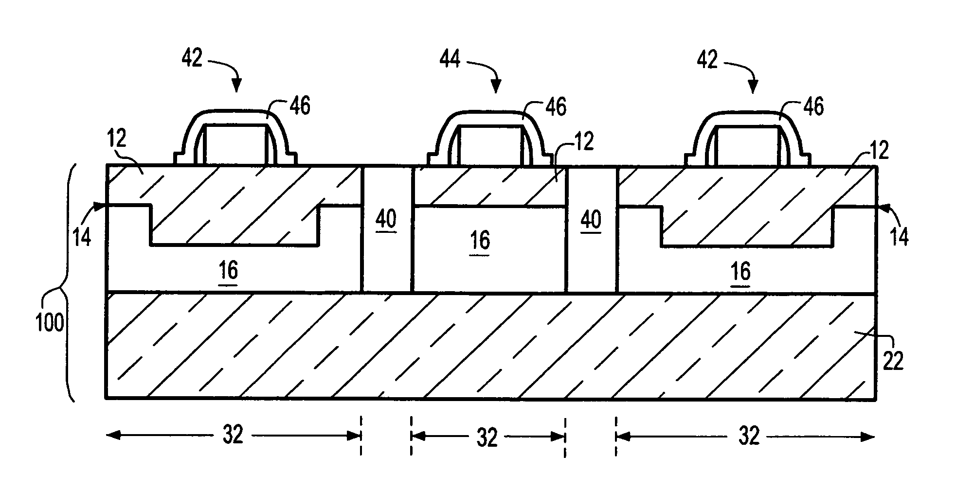
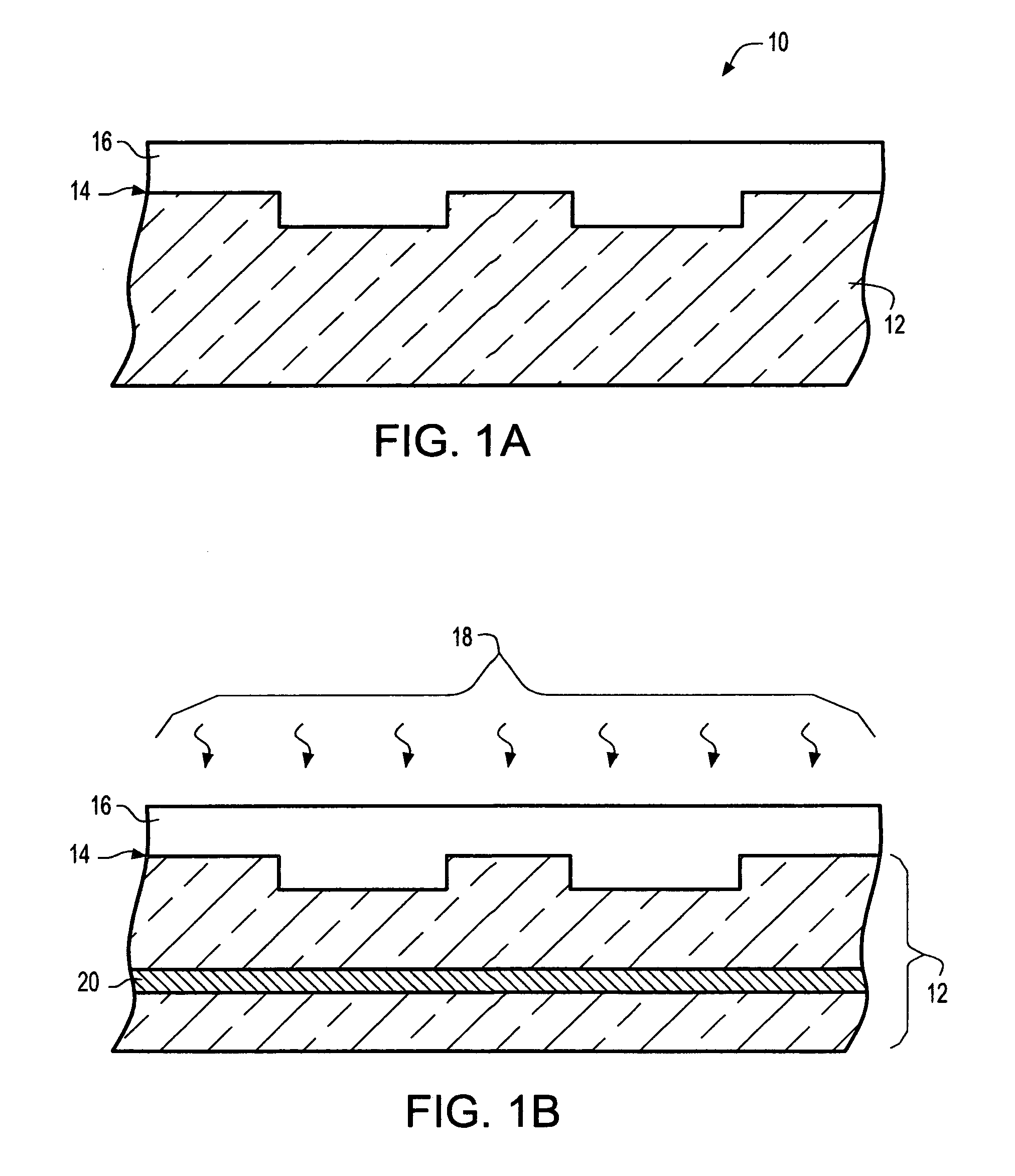
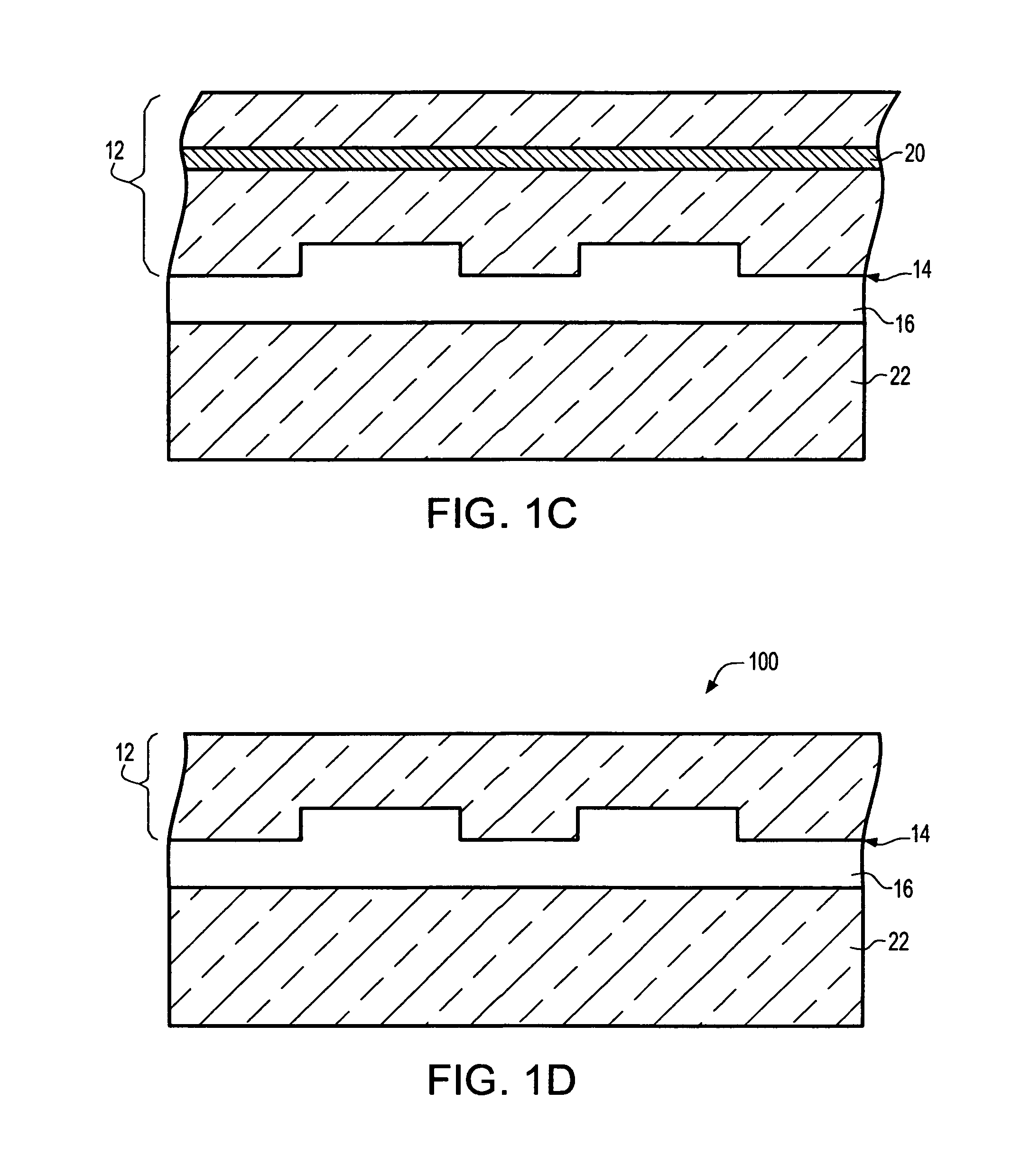
[0018]The present invention, which provides a semiconductor structure that includes a stress-inducing insulator separating an upper semiconductor layer from a bottom semiconductor layer in at least one portion of a wafer, will now be described in greater detail. It is noted that the drawings that accompany the present application are provided for illustrative purposes and thus they are not drawn to scale.

[0019]As stated above and in broad terms, the present invention provides a semiconductor structure that comprises an upper semiconductor layer and a bottom semiconductor layer, wherein said upper semiconductor layer is separated from said bottom semiconductor layer in at least one region by a stress-inducing insulator, said stress-inducing insulator exerts a strain on the upper semiconductor layer. In accordance with the present invention, the stress-inducing insulator may have a preselected geometry which is determined by a first prepatterned semiconductor layer. This broad aspect ...


PUM


Abstract

The present invention provides a semiconductor structure that includes a high performance field effect transistor (FET) on a semiconductor-on-insulator (SOI) in which the insulator thereof is a stress-inducing material of a preselected geometry. Such a structure achieves performance enhancement from uniaxial stress, and the stress in the channel is not dependent on the layout design of the local contacts. In broad terms, the present invention relates to a semiconductor structure that comprises an upper semiconductor layer and a bottom semiconductor layer, wherein said upper semiconductor layer is separated from said bottom semiconductor layer in at least one region by a stress-inducing insulator having a preselected geometric shape, said stress-inducing insulator exerting a strain on the upper semiconductor layer.

Description

FIELD OF THE INVENTION[0001]The present invention relates to a semiconductor structure and methods of fabricating the same. More particularly, the present invention relates to a semiconductor structure including a stress-inducing insulator as a buried insulator of a semiconductor-on-insulator (SOI) substrate. By using a stress-inducing insulator as the buried insulator a strain can be exerted on the top semiconductor, i.e., SOI, layer.BACKGROUND OF THE INVENTION[0002]It is widely regarded that conventional semiconductor device scaling has ‘run-out’ of steam. Therefore, novel semiconductor device performance enhancements are necessary to continue to meet performance targets. Many performance enhancements attempt to utilize the effect that is generally referred to by those skilled in the art as “strained silicon”—that is, by applying a stress to the silicon lattice in the channel that the carrier mobility is enhanced. The enhanced carrier mobility, in turn, provides a substantial impr...

Claims


Application Information

Patent Timeline
Patent Type & Authority Patents(United States)
IPC IPC(8): H01L29/06
CPCH01L21/76254H01L27/1203H01L27/1207H01L29/7846H01L29/78
Inventor HOLT, JUDSON R.OUYANG, OIGING C.
Owner GLOBALFOUNDRIES INC
Why Eureka
Try Eureka