
Methods of fabricating light emitting diodes that radiate white light

a technology of light-emitting diodes and white light, which is applied in the direction of manufacturing tools, polycrystalline material growth, crystal growth process, etc., can solve the problems of reducing the lifetime of light-emitting diodes, limiting the use of solid-state white light sources, and significant complicating the packaging process

Inactive Publication Date: 2008-07-01
ALLEGIS TECH
View PDF21 Cites 17 Cited by
  • Summary
  • Abstract
  • Description
  • Claims
  • Application Information

AI Technical Summary

Problems solved by technology

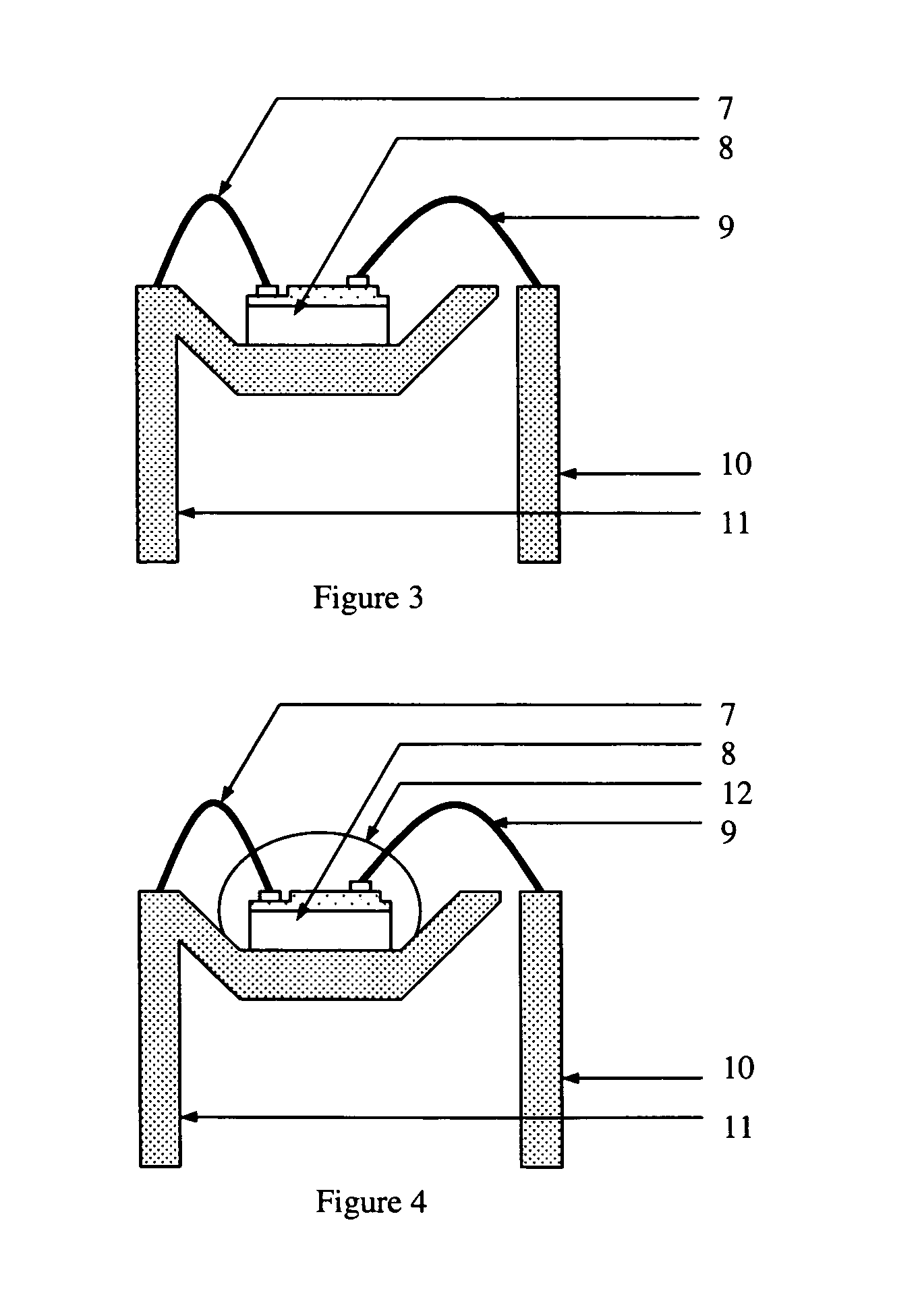
This conventional approach of applying the phosphor during packaging significantly complicates the packaging process, and limits the use of solid state white light sources.
Furthermore, over time the phosphor layer often interacts with the GaN chip, the wire bonds, or the epoxy used to encapsulate the LED package, resulting in degradation over time and reduced lifetimes.

Method used


Image

  • Methods of fabricating light emitting diodes that radiate white light
  • Methods of fabricating light emitting diodes that radiate white light
  • Methods of fabricating light emitting diodes that radiate white light

Examples


Embodiment Construction

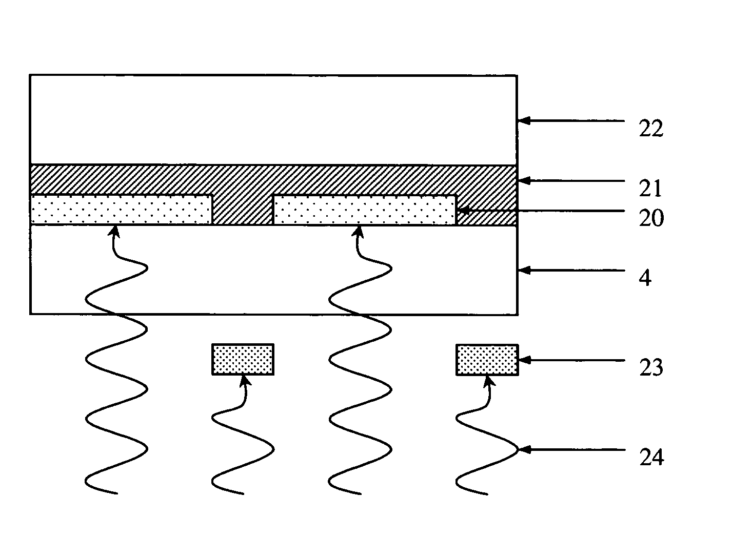
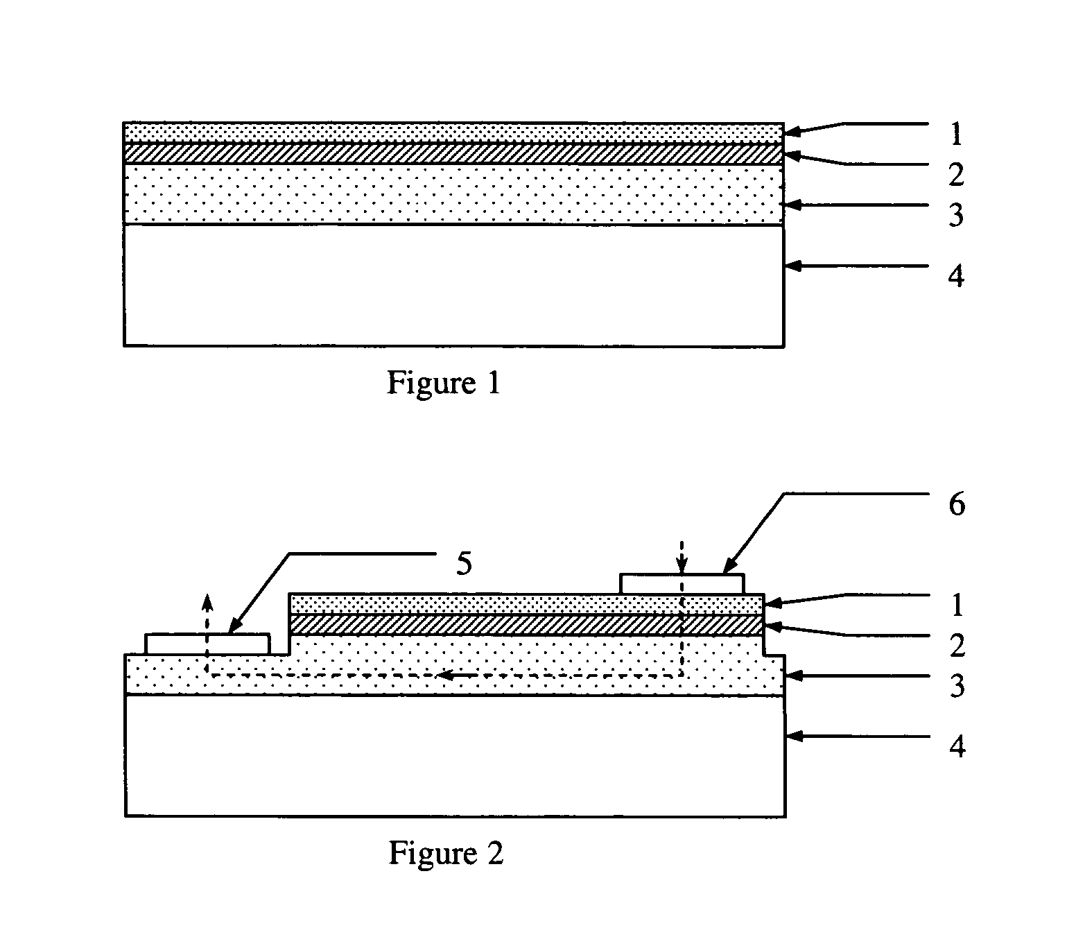
[0023]In one embodiment, GaN epitaxial films grown for LED applications consist of three main, sequentially grown layers (FIG. 1), each of which can be further subdivide into numerous additional layers. The main layers consist of a moderately conductive p-doped GaN layer (1), a light emitting InGaN quantum well (either single or multiple) layer (2), and a conductive n-doped GaN layer (3). Due to the rectifying nature of the GaN p-n junction, such a GaN film can only conduct electrical current from the p-layer (1), through the quantum well (QW) layer (2), into the n-layer (3), not in the other direction. Light will emit from the QW layer only if sufficient current is passed through it, as described above. Consequently, a GaN LED device requires a contact pad to both the n- and p-layers (1,3) through which to deliver this activating current.

[0024]In the conventional GaN on sapphire LED (FIG. 2), some of the GaN must be removed to make contact to the n-layer (3) via the n-pad (5). This...


PUM

PropertyMeasurementUnit
currentaaaaaaaaaa
lifetimesaaaaaaaaaa
depositionaaaaaaaaaa

Abstract

A method for fabricating an LED that radiates white spectrum light. A phosphor that radiates a white spectrum after excitation in the blue or UV spectrum is uniformly deposited onto a GaN epitaxial wafer prior to die separation and packaging. This allows wafer-level processing and probing of white LEDs and produces true white LED chips.

Description

CROSS REFERENCE TO RELATED APPLICATIONS[0001]The present application is a continuation of U.S. Patent Application Ser. No. 10 / 892,525, filed on Jul. 14, 2004, which claims priority from U.S. Provisional Patent Applications including the following serial numbers: Ser. No. 60 / 492,720 field Aug. 4, 2003; Ser. No. 60 / 489,350 filed Jul. 22, 2003; Ser. No. 60 / 487,896 filed Jul. 14, 2003; Ser. No. 60 / 492,713 filed Aug. 4, 2003; and Ser. No. 60 / 487,417 filed Jul. 14, 2003. The disclosure of these applications is incorporated herein by reference.BACKGROUND OF THE INVENTION[0002]1. Field of the Invention[0003]The present invention relates generally to the field of high power light emitting diodes, and more particularly to white gallium nitride diodes.[0004]2. Description of the Prior Art[0005]Gallium nitride (GaN) based light emitting diodes (LEDs) are an important source of solid state lighting in the UV through green portion of the spectrum. A white spectrum LED cannot be generated directly...

Claims


Application Information

Patent Timeline
Patent Type & Authority Patents(United States)
IPC IPC(8): H01L21/00C30B1/00H01LH01L21/20H01L21/36H01L33/00H01L33/64
CPCB23K26/409C30B25/02C30B29/406H01L33/0079H01L33/641H01L2224/48091H01L2224/48247H01L2924/10253H01L2924/12041H01L2224/48257H01L2924/00014H01L2924/00B23K26/40B23K2103/172H01L33/0093
Inventor URBANEK, WOLFRAM
Owner ALLEGIS TECH
Learn More