Compound semiconductor particles and production process therefor

a technology of semiconductor particles and production processes, applied in the field of compound semiconductor particles, can solve the problems of insufficient performance, lack of heat resistance, and easy oxidation of the surface of the surface of the semiconductor particles, and achieve the effects of excellent performance, extreme ease, and good productivity

Inactive Publication Date: 2008-08-05
KOBAYASHI MASAKAZU +1
View PDF20 Cites 4 Cited by
  • Summary
  • Abstract
  • Description
  • Claims
  • Application Information

AI Technical Summary

Benefits of technology

[0018]The present invention can provide compound semiconductor particles that can display more excellent performance in functions peculiar to the compound semiconductor (e.g. luminosity and luminescence efficiency). Also, the present invention can provide a production process for obtaining such compound semiconductor particles with economy, good productivity, and extreme ease.

Problems solved by technology

However, the compound semiconductor particles generally have a problem such that, if the compound semiconductor particles are quantum-sized, then they become unable to sufficiently perform their peculiar functions, for the reason such that: the particles are lacking in heat resistance, and their surfaces become more easily oxidized.
Thus, it is thought that: the particles are lacking in stability and durability and are very difficult to put to practical use.
In addition, in the case where the particles are fined to thereby be quantum-sized, it becomes more and more difficult to maintain a favorable monodispersed state.
However, unless the compound semiconductor particles are in such a favorable monodispersed state, for example, there is a problem that: their luminosity greatly decreases, and further there is a problem that the properties such as luminescence greatly vary also with the kinds of dispersants as used for dispersing the particles.
However, as to this method, the compound semiconductor particles which are inherently lacking in chemical durability (e.g. oxidation resistance) and thermal durability are merely treated with the similar compound semiconductor.
Therefore, even if the properties are temporarily enhanced, there is a problem of lacking the practicability after all.
However, as to this method, the attachment of the oxide particles to the compound semiconductor particles needs a heat-treatment step at a high temperature after the attachment-treatment step.
Therefore, there are problems such that: the movement of substances and the defectiveness occur during this heating at the high temperature to greatly deteriorate the luminescence property; and there are economical disadvantages of increasing such as treatment costs, and it is necessary to involve a complicated treatment step, so the productivity is inferior.
However, these methods, for example, have the following prior problems: the chemical and thermal stabilities are insufficient; the monodispersibility is so inferior that the excellent fluorescence property as expected by the nano-sizing cannot sufficiently be displayed; and also, the economy is poor, and the productivity is inferior.

Method used


Image

  • Compound semiconductor particles and production process therefor
  • Compound semiconductor particles and production process therefor
  • Compound semiconductor particles and production process therefor

Examples


example 1

[0195]A stainless-steel (SUS316)-made pot of 120 mL in capacity was charged with 270 parts of stainless-steel (SUS316)-made balls having a diameter of 3.18 mmφ (as balls for polish-pulverization), 13 parts of CdSe (as the compound semiconductor), and 4 parts of heptane (as the solvent), and then the pot was tightly shut. Incidentally, the pot as used was the shape of a column having a sectional diameter of 50 mm, and its bottom had a curved semispherical face having a radius of curvature of 25 mm and being convex outward of the pot.

[0196]This pot was set to a ball mill apparatus to make revolution at a set revolution rate of the pot of 298 rpm and a set revolution rate of the disk of 139 rpm for 80 hours, thus carrying out the polish-pulverization (hereinafter referred to as polish-pulverization treatment).

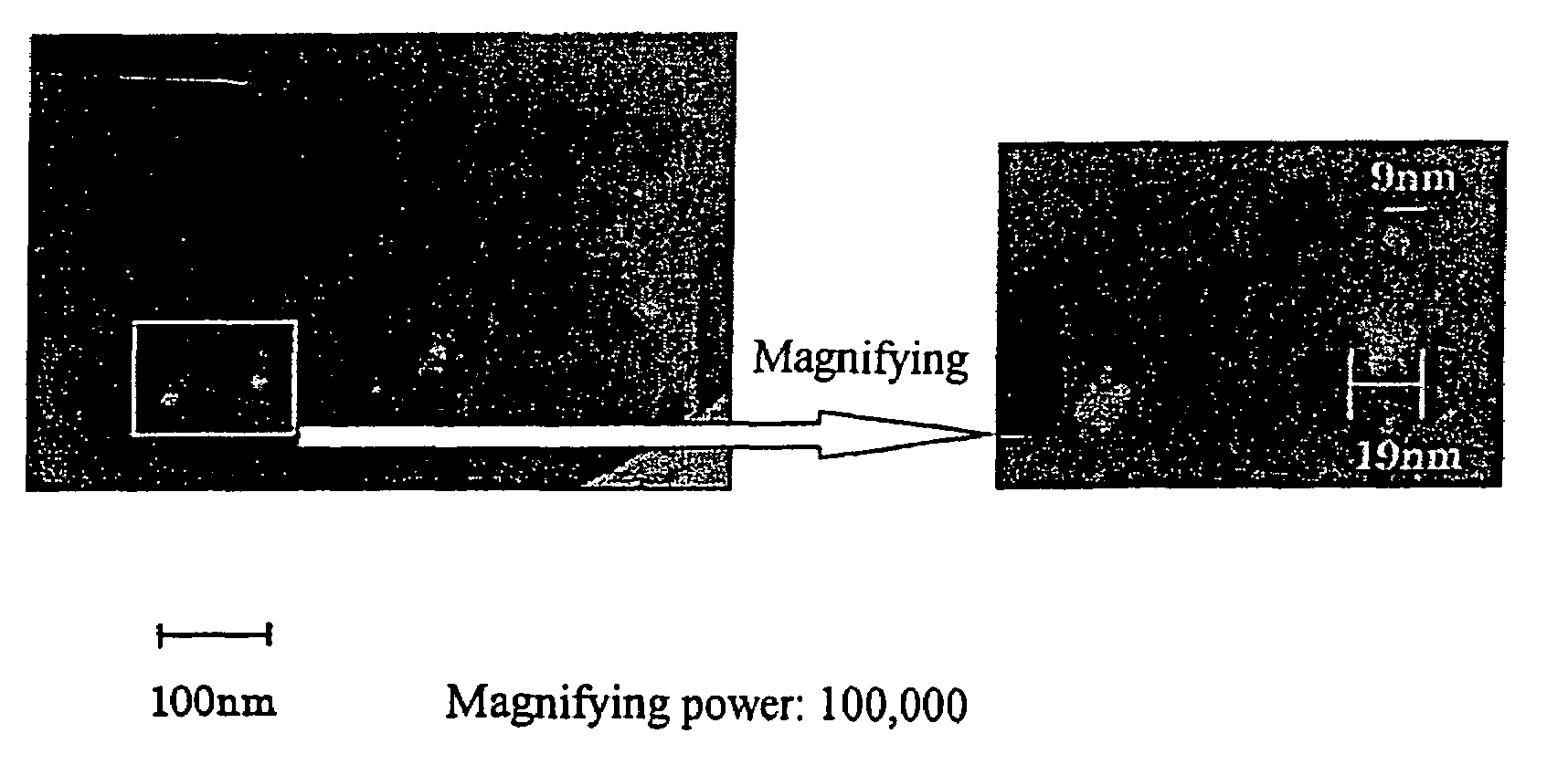
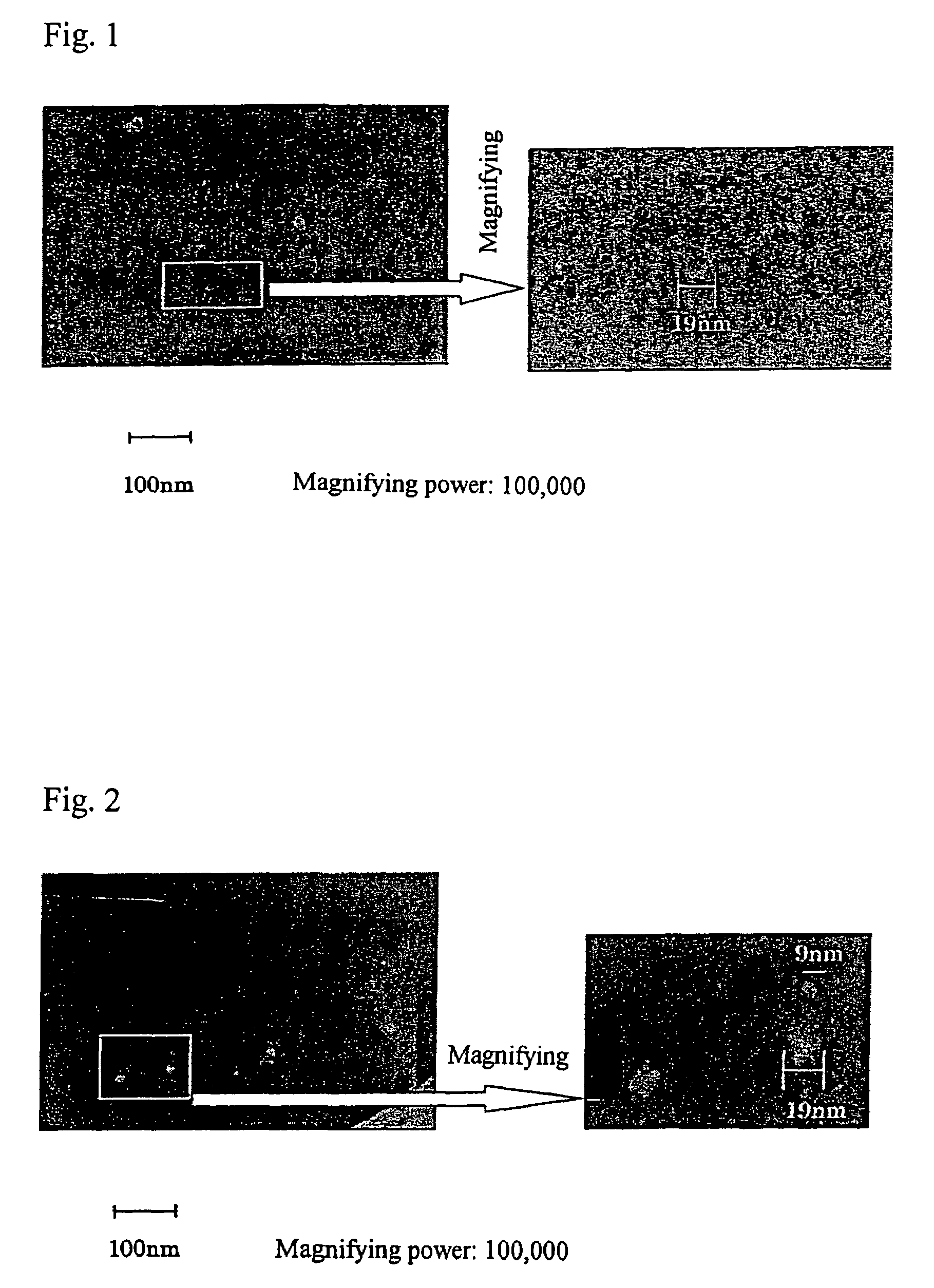
[0197]After the polish-pulverization treatment, there was obtained a dispersion (1a) of compound semiconductor particles by filtrating the contents as obtained in the pot. As a re...

example 2

[0199]The same pot as used in Example 1 was charged with 65 parts of stainless-steel (SUS316)-made balls having a diameter of 5 mmφ (as balls for polish-pulverization), 5 parts of CdSe (as the compound semiconductor), and 3 parts of methanol (as the solvent), and then the pot was tightly shut.

[0200]This pot was set to a ball mill apparatus to make revolution at a set revolution rate of the pot of 229 rpm and a set revolution rate of the disk of 107 rpm for 40 hours, thus carrying out the polish-pulverization treatment.

[0201]After the above treatment (revolution for 40 hours), there were taken out the stainless-steel (SUS316)-made balls for the polish-pulverization having a diameter of 5 mmφ, and then instead thereof stainless-steel (SUS316)-made balls for polish-pulverization having a diameter of 3 mmφ were charged into the pot. Then, the revolution was made for 52 hours under the same revolution rate conditions as of the preceding treatment, thus carrying out the polish-pulverizati...

example 3

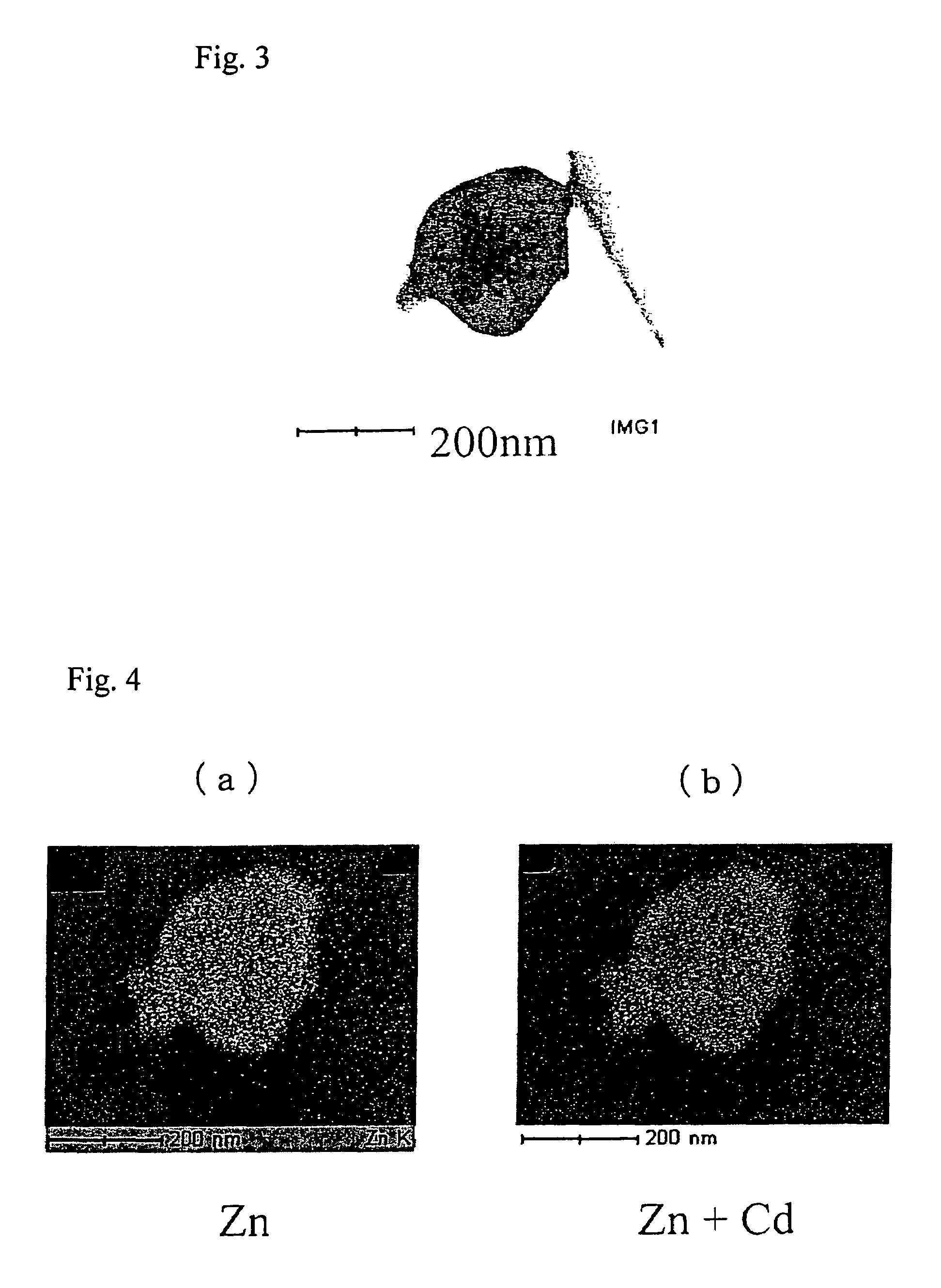
[0204]There was obtained a dispersion (3a) of compound semiconductor particles in the same way as of Example 2 except to replace the 5 parts of CdSe with 5 parts of ZnS. As a result of observation of the dispersion (3a) with a TEM, it was confirmed that fine ZnS particles (compound semiconductor particles) having an average particle diameter of 0.03 μm were formed in the dispersion (3a) wherein a portion of the ZnS particles were fine ZnS particles having particle diameters of not larger than 10 nm.


PUM

PropertyMeasurementUnit
particle diametersaaaaaaaaaa

Abstract

There are provided: compound semiconductor particles that can display more excellent performance in functions peculiar to the compound semiconductor (e.g. luminosity and luminescence efficiency); and a production process for obtaining such compound semiconductor particles with economy, good productivity, and ease.Compound semiconductor particles, according to the present invention, are characterized by comprising body particles and a metal oxide, wherein the body particles have particle diameters of smaller than 1 μm and are covered with the metal oxide and include a compound semiconductor including an essential element combination of at least one element X selected from the group consisting of C, Si, Ge, Sn, Pb, N, P, As, Sb, S, Se, and Te and at least one metal element M that is not identical with the element X, and wherein the metal oxide is a metal oxide to which an acyloxyl group is bonded.

Description

[0001]This is the U.S. national phase of International Application No. PCT / JP2003 / 010818, filed Aug. 27, 2003, which claims priority from Japanese Patent Application No. 2003-086310 filed Mar. 26, 2003 and Japanese Patent Application No. 2002-262061 filed Sept. 6, 2002.TECHNICAL FIELD[0002]The present invention relates to compound semiconductor particles and a production process therefor.BACKGROUND ART[0003]It has hitherto been known that: particles including a so-called compound semiconductor such as ZnS and CdSe (also including compound semiconductors doped with such as Ag and Mn) (compound semiconductor particles) have various useful functions such as of being able to emit fluorescence by irradiating the particles with ultraviolet rays and / or electron beams as excitation sources or applying a voltage to the particles (e.g. U.S. Pat. No. 5,455,489). In addition, in recent years, as to compound semiconductor particles including such as CdSe and Mn-doped ZnS, it is being verified on...

Claims


Application Information

Patent Timeline
Patent Type & Authority Patents(United States)
IPC IPC(8): H01L21/469C01B19/04C01B17/42C01B19/00C01B25/08C01B25/45C01B31/36C01F17/00C01G9/00C01G9/08C01G25/00C09K11/02C09K11/56C09K11/62C09K11/88
CPCB82Y30/00C09K11/883C01B19/002C01B19/007C01F17/0037C01F17/0093C09K11/025C09K11/565C09K11/623C01B17/42C01P2002/60C01P2002/84C01P2002/85C01P2004/04C01P2004/64C01P2004/80C01F17/38C01F17/294C01B19/04
Inventor KOBAYASHI, MASAKAZUTAKEDA, MITSUO
Owner KOBAYASHI MASAKAZU
Why Eureka
Try Eureka