Method of manufacturing a semiconductor device

a manufacturing method and semiconductor technology, applied in semiconductor devices, semiconductor/solid-state device details, electrical devices, etc., can solve the problems of high possibility of packaging defect such as peeling of semiconductor devices from wiring substrates, short length of soldered portions for external connection of each lead, etc., to improve packaging reliability of semiconductor devices and reduce the size of semiconductor devices

Active Publication Date: 2008-08-12
RENESAS ELECTRONICS CORP
View PDF4 Cites 36 Cited by
  • Summary
  • Abstract
  • Description
  • Claims
  • Application Information

AI Technical Summary

Benefits of technology

[0012]Reduction in size (planar size) of the QFN type semiconductor device can be attained by shortening the distance between side faces of a semiconductor chip and side faces of a resin sealing body. However, for shortening the distance, it is necessary to shorten the length of each lead, with the result that the length of a terminal portion (soldered portion) for external connection of each lead also becomes short. Consequently, the area of bonding between each lead and a solder material at the time of soldering the semiconductor device to a wiring substrate becomes small and the bonding strength between electrode pads (lands, foot print) formed on a wiring substrate and the leads of the semiconductor device becomes low, so that the possibility of occurrence of a packaging defect such as peeling of the semiconductor device from the wiring substrate becomes high.
[0030]According to the present invention it is possible to attain the reduction in size of the semiconductor device.

Problems solved by technology

However, for shortening the distance, it is necessary to shorten the length of each lead, with the result that the length of a terminal portion (soldered portion) for external connection of each lead also becomes short.
Consequently, the area of bonding between each lead and a solder material at the time of soldering the semiconductor device to a wiring substrate becomes small and the bonding strength between electrode pads (lands, foot print) formed on a wiring substrate and the leads of the semiconductor device becomes low, so that the possibility of occurrence of a packaging defect such as peeling of the semiconductor device from the wiring substrate becomes high.

Method used


Image

  • Method of manufacturing a semiconductor device
  • Method of manufacturing a semiconductor device
  • Method of manufacturing a semiconductor device

Examples


first embodiment

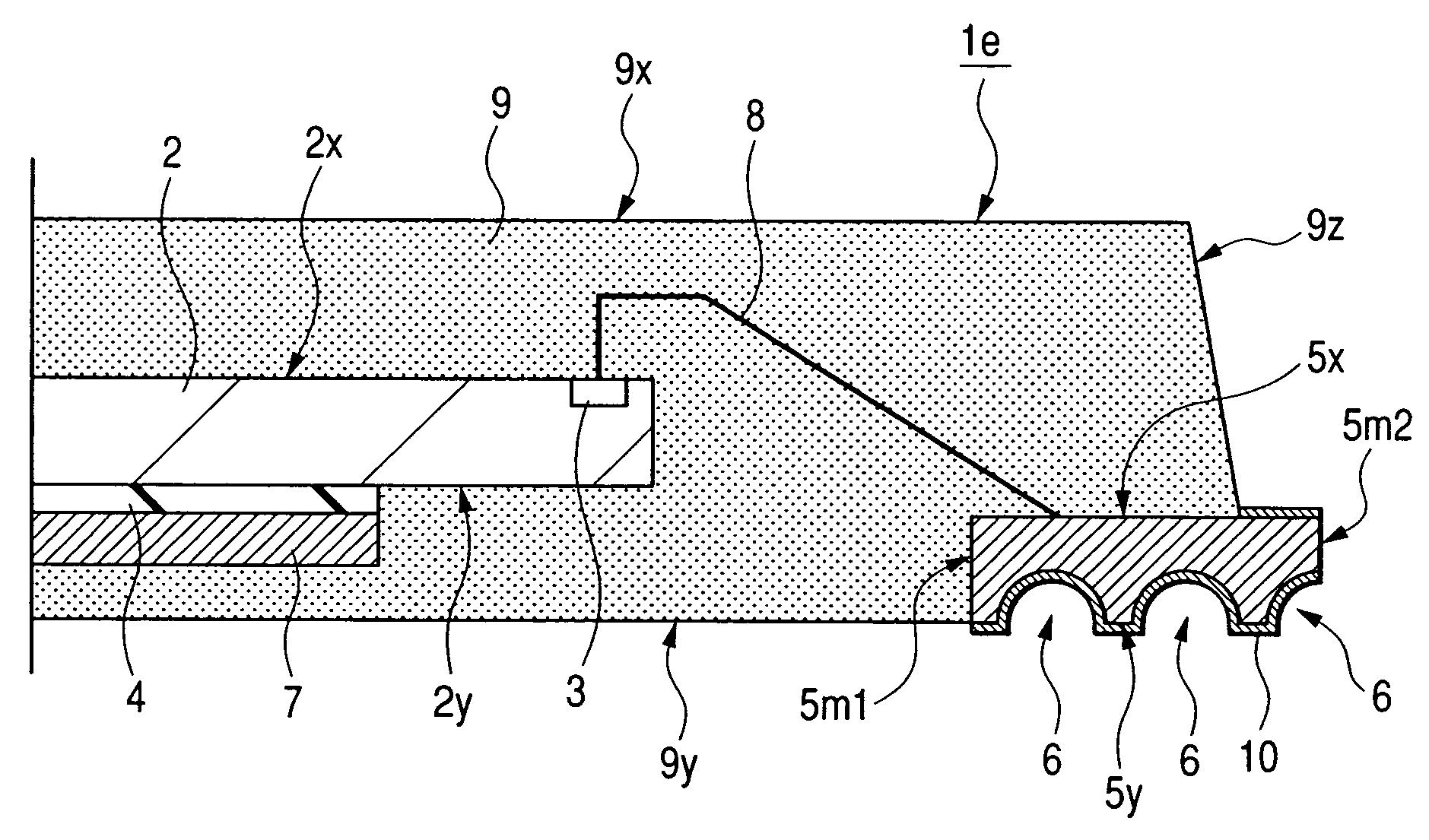
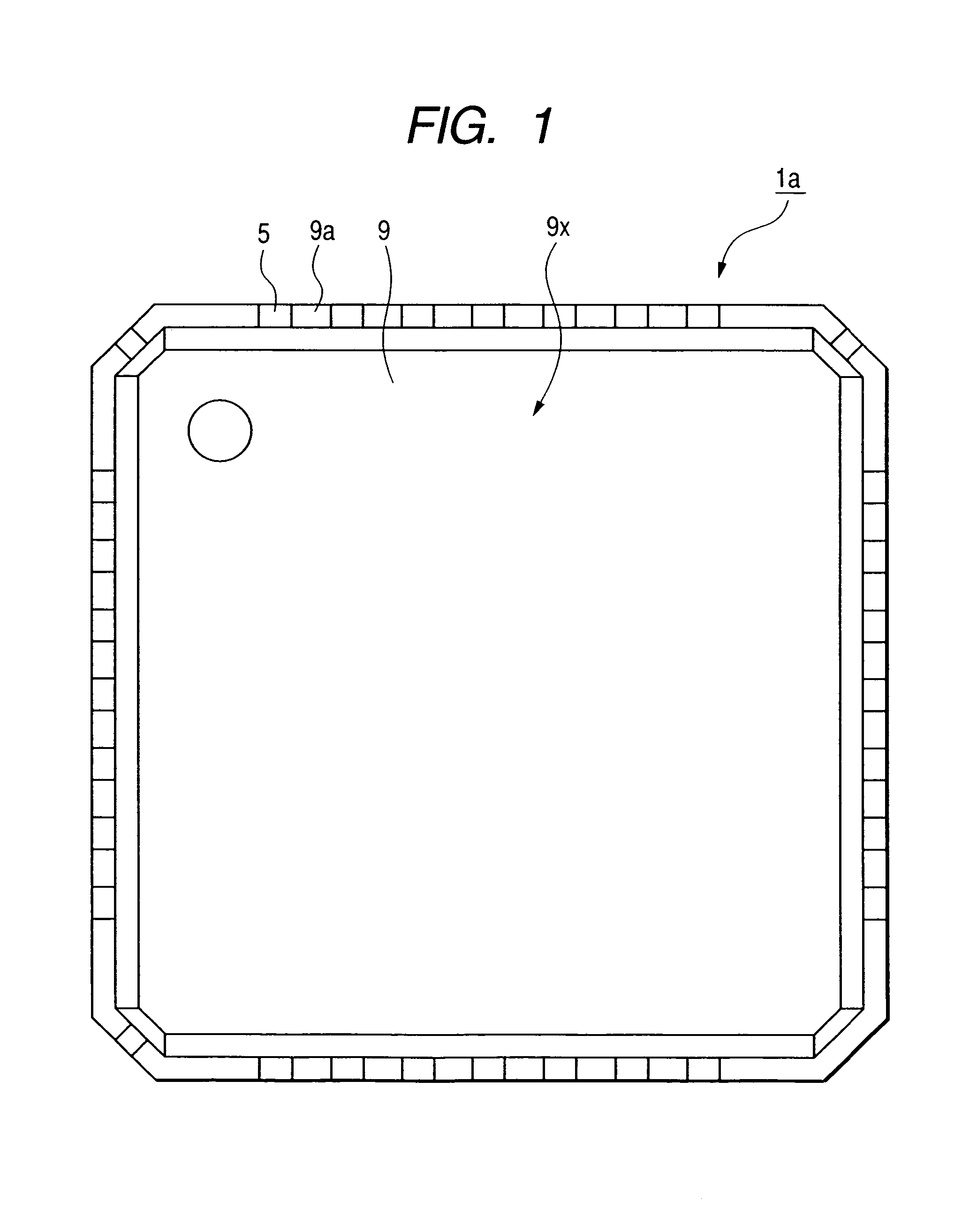
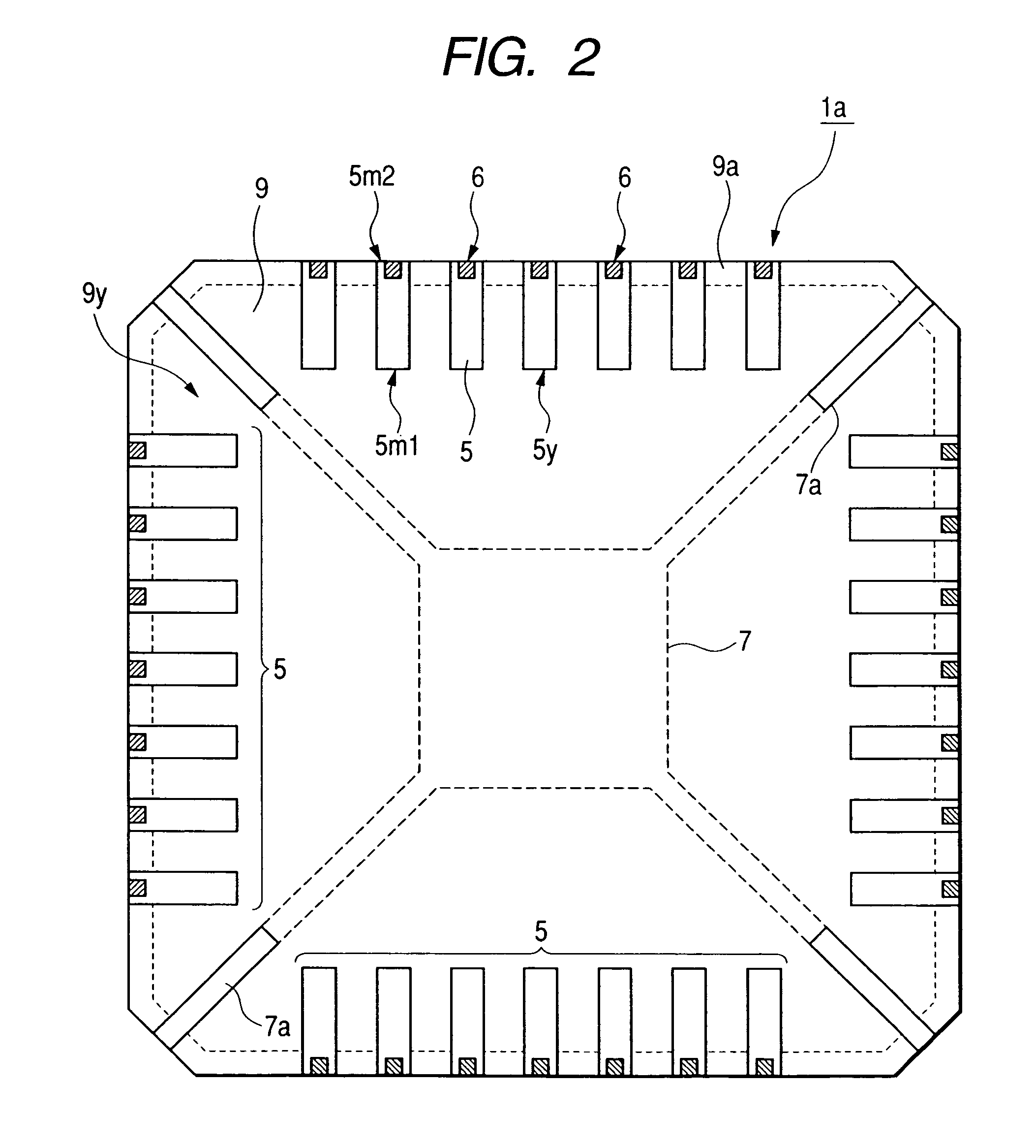
[0069]In this first embodiment, reference will be made to an example of application of the present invention to a QFN type semiconductor device as a non-leaded semiconductor device in which leads are partially exposed as terminal portions for external connection to a back surface of a resin sealing body.

[0070]FIGS. 1 to 18 are related to a semiconductor device according to a first embodiment of the present invention, of which FIG. 1 is a schematic plan view (top view) showing an appearance structure of the semiconductor device, FIG. 2 is a schematic bottom view (underside view) thereof, FIG. 3 is a partially enlarged, schematic bottom view (underside view) of FIG. 2, FIGS. 4(a) and 4(b) show an internal structure of the semiconductor device, of which FIG. 4(a) is a schematic plan view with an upper portion of a resin sealing body removed and FIG. 4(b) is a schematic sectional view taken along line a-a in FIG. 4(a), FIG. 5 is a partially enlarged, schematic sectional view of FIG. 4(b...

second embodiment

[0122]In this second embodiment, a description will be given of an example in which the present invention is applied to a semiconductor device including leads provided with anti-dislodgment means.

[0123]FIG. 19 is a schematic sectional view showing a part of an internal structure of the semiconductor device according to this second embodiment of the present invention, and FIG. 20 is a schematic bottom view (underside view) of a lead shown in FIG. 19.

[0124]As shown in FIG. 19, the semiconductor device of this second embodiment, indicated at 1b, is basically of the same construction as the previous first embodiment, with a difference lying in the construction of each lead 5.

[0125]As shown in FIGS. 19 and 20, each lead 5 has, in addition to the above construction, a third surface Syl positioned on the side opposite to the first surface 5x and closer to the first surface 5x than the second surface 5y. The third surface 5yl is contiguous to the first end face 5m1, is positioned within the...

third embodiment

[0128]In this third embodiment, a description will be given of a first modification in which the shape of a recessed portion formed in each lead is changed.

[0129]FIG. 21 is a schematic sectional view showing a part of an internal structure of a semiconductor device according to a third embodiment of the present invention and FIG. 22 is a schematic bottom view (underside view) of a lead shown in FIG. 21.

[0130]The recessed portion 6 in the first embodiment is formed outside a side face 9z of the resin sealing body 9. As shown in FIG. 21, a recessed portion 6 used in this third embodiment is formed both outside and inside a side face 9z of the resin sealing body 9. As shown in FIG. 22, the recessed portion 6 is exposed from the second end face 5m2 of each lead 5 and is spaced away from both side faces opposed to each other in the width direction of the lead 5 and also from the first end face 5m1. According to such a construction, in comparison with the first embodiment, when the semico...


PUM


Abstract

A semiconductor device improved in packaging reliability is disclosed. Each of leads used in the semiconductor device has a first surface positioned between a main surface of a resin sealing body and a back surface opposite to the main surface of the resin sealing body, a second surface positioned on the side opposite to the first surface and exposed from the back surface of the resin sealing body, a first end face positioned on a semiconductor chip side, a second end face positioned on the side opposite to the first end face and exposed from a side face of the resin sealing body, and a recessed portion depressed from the second surface to the first surface side and contiguous to the second end face, the second surface and an inner wall surface of the recessed portion being covered with a plating layer which is higher in solder wettability than the second end face of each of the leads.

Description

CROSS-REFERENCE TO RELATED APPLICATION[0001]The present application claims priority from Japanese patent application No. 2003-430092 filed on Dec. 25, 2003, the content of which is hereby incorporated by reference into this application.BACKGROUND OF THE INVENTION[0002]The present invention relates to a semiconductor device and a method of manufacturing the same. Particularly, the present invention relates to a technique applicable effectively to a non-leaded semiconductor device.[0003]As semiconductor devices in which a semiconductor chip with an integrated circuit mounted thereon is sealed with resin, those of various package structures have been proposed and are available commercially. Among them, for example a semiconductor device called QFN (Quad Flat Non-Leaded Package) type is known. The QFN type semiconductor device has a package structure in which leads connected electrically to electrodes formed on a semiconductor chip are exposed as external connecting terminals from a bac...

Claims


Application Information

Patent Timeline
Patent Type & Authority Patents(United States)
IPC IPC(8): H01L21/00H01L21/44H01L23/28H01L21/48H01L21/56H01L21/60H01L23/31H01L23/48H01L23/495H01L23/50H01L23/52
CPCH01L21/565H01L23/49548H01L24/97H01L23/3107H01L24/48H01L2224/32014H01L2224/32245H01L2224/48095H01L2224/48247H01L2224/49171H01L2224/73265H01L2224/92247H01L2224/97H01L2924/01027H01L2924/01029H01L2924/01033H01L2924/01078H01L2924/01079H01L2924/01082H01L2924/14H01L2924/1532H01L2924/19043H01L24/49H01L2924/01005H01L2924/01006H01L2224/45144H01L2924/12041H01L2224/85H01L2224/83H01L2924/00H01L2224/45015H01L2924/181H01L2924/00014H01L24/45H01L2224/05554H01L2924/00012H01L2224/05599H01L23/52
Inventor FUKAYA, SYUUDAISHINYA, TOSHIYUKIHASEBE, HAJIME
Owner RENESAS ELECTRONICS CORP
Why Eureka
Try Eureka