Single exposure of mask levels having a lines and spaces array using alternating phase-shift mask

a phase shift mask and single exposure technology, applied in the field of optical lithography methods, can solve the problems of reducing the depth of focus, deteriorating the contrast of the pattern formed on the wafer, and neither alternative is practical at these smaller dimensions

Inactive Publication Date: 2008-08-19
INFINEON TECH AG +1
View PDF2 Cites 7 Cited by
  • Summary
  • Abstract
  • Description
  • Claims
  • Application Information

AI Technical Summary

Benefits of technology

[0016]In accordance with an aspect of the invention, a lithographic mask pattern is provided that includes at least one adjacent pair of spaces and a first substantially opaque feature disposed between the adjacent pair of spaces. One space of the adjacent pair of spaces transmits light with an opposite phase shift to that of another space of the adjacent pair of spaces. A connector region is incorporated in the mask pattern between ends of the first substantially opaque feature and a second substantially opaque feature such that the adjacent pair of spaces do not intersect one another. A portion of the mask pattern is located atop a previously defined trench region such that the trench region prevents the first substantially opaque feature and the second substantially opaque feature from shorting to one another.
[0019]In accordance with a still further aspect of the invention, a lithographic mask pattern of a mask level is provided. The mask pattern includes an array region comprised of at least one lines and spaces pattern. One space of each adjacent pair of spaces of the lines and spaces pattern transmits light with an opposite phase shift to that of another space of the adjacent pair of spaces. A respective landing pad region, is incorporated in the lines and spaces pattern at an end of at least two lines of the lines and spaces pattern such that a further mask pattern of the mask level may be aligned thereto. Adjacent pairs of spaces of the lines and spaces pattern are thereby prevented from intersecting one another on the mask pattern.

Problems solved by technology

In both methods, however, as the lines and spaces patterns that are to be printed approach submicron sizes, the contrast of the patterns formed on the wafer deteriorates, and the depth of focus decreases.
As a result, neither alternative is practical at these smaller dimensions.
The segmented line mask patterns that define the features likewise are smaller and become increasingly difficult to print because of line shortening effects.
Moreover, the active area, bit line and word line mask patterns not only include lines and spaces, which are used in the array areas of these levels, but also include small isolated spaces, which likewise are difficult to print because of the limited size of the open areas that can be printed using the masks, as well as larger sized features used in the support circuitry regions.
The phase-shifting mask diffracts the light transmitted by the mask pattern and causes it to interfere destructively or constructively based on the location on the mask pattern, thereby increasing the depth of focus and allowing for the printing of finer lines and spaces patterns.
The dark areas of the mask typically transmit the incident light at a reduced intensity but with a 180 degrees phase shift relative to the clear areas of the mask so that the light transmitted by the dark areas interfere with the light transmitted by the clear areas.
The use of attenuated phase-sift masks, however, requires off-axis illumination (OAI) and thus cannot be carried out using standard projection printing systems.
The light diffracted into the line regions between the clear regions interfere destructively to improve the image contrast as well as the resolution and depth of focus.
However, the patterns printed using such a mask have lines that are shorted to each other and thus would require a second exposure using another mask pattern, typically a standard chrome-on-glass mask pattern, to remove the segments creating the shorts.
The double exposure required to incorporate an alternating phase-shift mask pattern requires an additional mask-to-mask alignment step that increases the possibility of introducing alignment errors as well as increasing fabrication costs and personnel expense.
The added mask level also increases the possibility of introducing defects.
As a result, the use of alternating phase-shift masks are limited to mask levels having only array type patterns that require only a single exposure or to mask levels in which the added cost of a double exposure step cannot be avoided.

Method used


Image

  • Single exposure of mask levels having a lines and spaces array using alternating phase-shift mask
  • Single exposure of mask levels having a lines and spaces array using alternating phase-shift mask
  • Single exposure of mask levels having a lines and spaces array using alternating phase-shift mask

Examples


Embodiment Construction

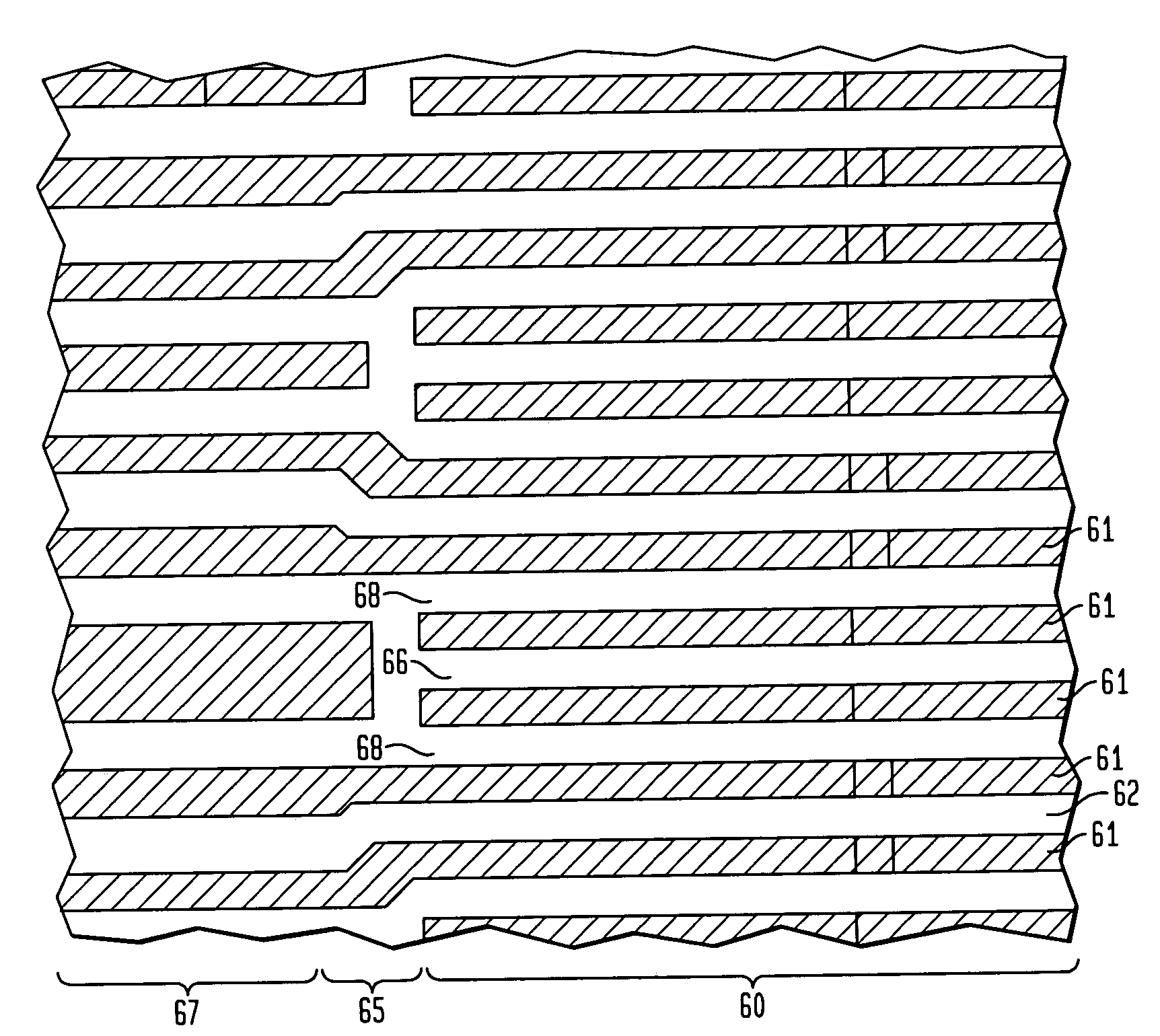
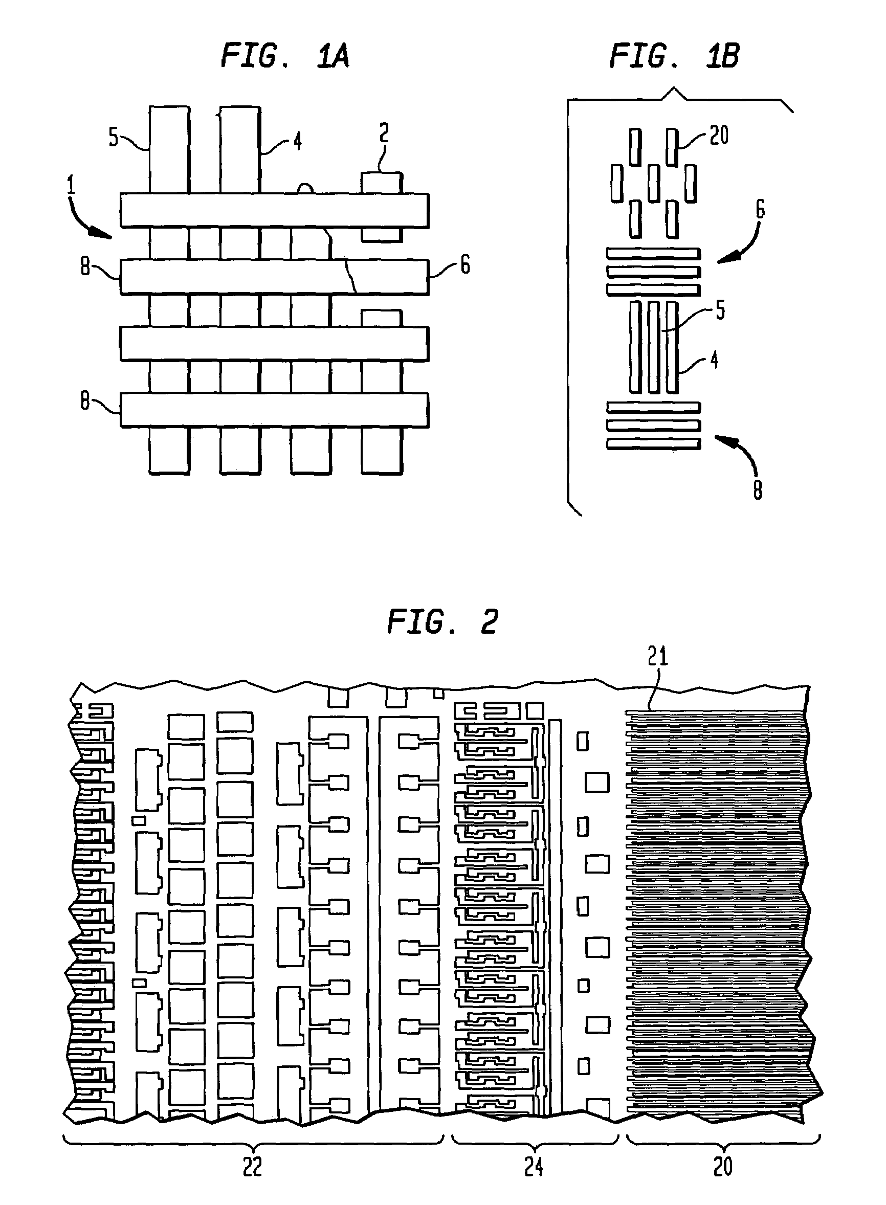
[0036]FIGS. 1A and 1B illustrate, in plan view, a known DRAM memory cell array comprised of plural memory cells, typically a trench-based DRAM cell array known as an eight square feature or 8F2 cell. Examples of such DRAM cells and processes for the fabrication are described in U.S. application Ser. No. 09 / 888,202, filed Jun. 22, 2001, the disclosure of which is incorporated herein by reference.

[0037]FIG. 1A shows several mask patterns of the known memory cell array superimposed on one another. FIG. 1B shows each mask pattern of FIG. 1A separately, namely FIG. 1B represents the view of FIG. 1A at four different depths. The topmost pattern of FIG. 1B illustrates an arrangement of a plurality of deep trenches 20. The second pattern from the top in FIG. 1B illustrates the arrangement of the active areas 6 in which are formed the doped junctions used for connection to the pass transistors. The third pattern from the top illustrates the arrangement of the gate contact patterns or word li...


PUM

PropertyMeasurementUnit
phase shiftaaaaaaaaaa
active areaaaaaaaaaaa
areaaaaaaaaaaa

Abstract

An active area pattern is formed atop a deep trench pattern with a single exposure using an alternative phase-shift mask. To prevent adjacent spaces of opposite phase from intersecting one another at the ends of substantially opaque features of the active area pattern, one or more connectors are used to connect the ends of the substantially opaque patterns. Trench regions of the deep trench pattern are arranged such that the conduction path of the connectors are interrupted and prevent the lines from shorting to one another. Alternatively, a bit line pattern or a word line pattern having a lines and spaces array and a support region are printed with a single exposure using an alternating phase-shift mask. At one end of the array region, lines having a respective phase shift extend into the support region, and lines of the opposite phase shift are terminated. At the opposite end of the array, the lines that have the opposite phase shift extend into the support region, and the lines of having the respective phase shift are terminated.

Description

BACKGROUND OF THE INVENTION[0001]The present invention relates to photolithography methods and, more particularly, to optical lithography methods for forming fine-sized patterns on a wafer or other substrates, such as using a photolithographic mask and a projection lens.[0002]In existing projection systems used in optical photolithography, a quasi-monochromatic, spatially incoherent light source of wavelength λ is used to illuminate a photolithographic mask having various patterns, such as a periodic pattern of equally spaced lines. The illuminating beam is usually collimated to ensure a highly uniform intensity distribution at the plane of the mask, and an adjustable condenser stop is used to control the degree of coherence of the illuminating beam. The light is transmitted through the mask and collected by a projection lens which images the mask patterns onto a wafer located at the image projection plane, typically at a predetermined reduction ratio.[0003]In such projection system...

Claims


Application Information

Patent Timeline
Patent Type & Authority Patents(United States)
IPC IPC(8): G03F1/00G03C5/00G03F9/00H01L21/308H01L21/3213H01L21/8242H01L27/02
CPCG03F1/30H01L21/3083H01L27/10882H01L27/0207H01L27/1087H01L21/32139H10B12/0387H10B12/48
Inventor BUTT, SHAHIDBUKOFSKY, SCOTTDIVAKARUNI, RAMACHANDRARADENS, CARLELLIS, WAYNE
Owner INFINEON TECH AG
Why Eureka
Try Eureka