

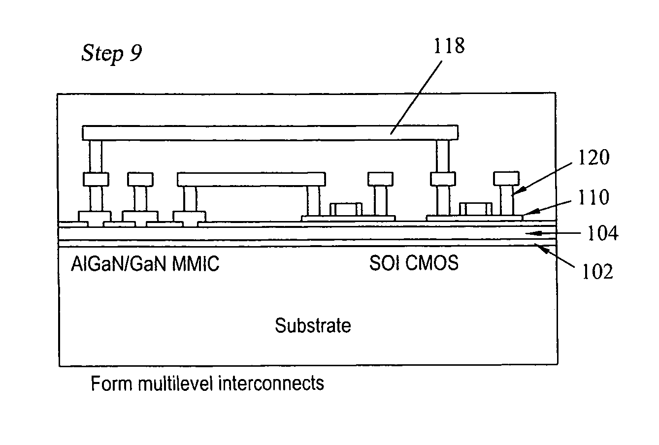
Method for integrating silicon CMOS and AlGaN/GaN wideband amplifiers on engineered substrates
a technology of wideband amplifiers and engineered substrates, which is applied in the direction of electrical equipment, semiconductor devices, semiconductor/solid-state device details, etc., can solve the problems of limited availability of suitable substrates for epitaxial growth, inability to achieve thermal dissipation properties that are necessary, and inability to meet the requirements of epitaxial growth
- Summary
- Abstract
- Description
- Claims
- Application Information
AI Technical Summary
Benefits of technology
Problems solved by technology
Method used
Image

Examples
examples
[0092]Two examples demonstrate the successful transfer of silicon to silicon carbide: (1) a silicon layer from a bulk silicon wafer to silicon carbide, and (2) a silicon layer from SOI to silicon carbide. Sonoscan images of the two are shown in FIGS. 16a and 16b. Bulk silicon, which is shown in FIG. 16a, was used for the first attempt in order to test the bonding process using the polished polycrystalline silicon carbide wafers. The center region shows small voids that can be attributed the planarization of the silicon layer. This particular set of wafers was thinned to approximately 100 μm.
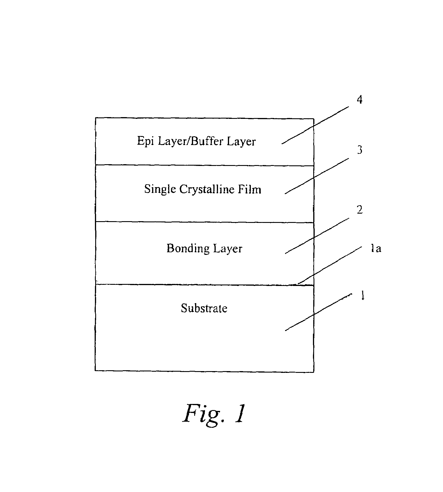
[0093]The second example of bonding entailed bonding an SOI wafer to polycrystalline silicon carbide. The sonoscan in FIG. 16b shows a uniform bond without voids. This wafer was annealed at 175° C. and thinned to the buried oxide layer. FIG. 17 shows a cross-section of the wafer pair shown in FIG. 16b. In FIG. 17, several layers can be distinguished: the polycrystalline silicon carbide substrate,...
PUM
| Property | Measurement | Unit |
|---|---|---|
| surface roughness | aaaaa | aaaaa |
| sizes | aaaaa | aaaaa |
| temperatures | aaaaa | aaaaa |
Abstract
Description
Claims
Application Information