Sensor device for interference and plasmon-waveguide/interference spectroscopy

a technology of interference and plasmon waveguide, applied in the field of optical sensor chips, can solve the problems of observing interference effects in both reflectance and transmittance modes, spr and cpwr spectroscopy, which are essentially limited to measurements, and achieve the effect of less risk of damage to the sensor

Inactive Publication Date: 2008-09-02
THE ARIZONA BOARD OF REGENTS ON BEHALF OF THE UNIV OF ARIZONA
View PDF6 Cites 10 Cited by
  • Summary
  • Abstract
  • Description
  • Claims
  • Application Information

AI Technical Summary

Benefits of technology

[0021]In a preferred embodiment, the sensor device includes an entrant medium in optical contact with a dielectric member (e.g., SiO2) that is about 100 microns in thickness. A sample solution is placed on the dielectric member and an incident angle of light below the critical angle for total internal reflection is reflected by and transmitted through the dielectric member, thereby producing observable interference effects in both reflectance and transmittance modes.
[0023]One of the main goals of this invention is the development of sensor devices that expand the observable range of optical phenomena that can be used to characterize molecules during spectroscopy. To that end, the invention further relates to a sensor unit for use in a system based on CPWR technology that includes a dielectric substrate having one or more sensing areas that contain at least one functional group supporting bi- or polyfunctional molecules capable of specific binding with molecules present in a sample analyte. Preferably, coupling between the bi- or polyfunctional molecules and the molecule(s) in the sample is selectively reversible such that the bi- or polyfunctional molecule-functionalized sensing areas can be regenerated, permitting repeated use of the functionalized sensor unit.
[0024]The sensor of the present invention differs from previous SPR and CPWR sensors in several key respects. First, the invention features a dielectric member that is approximately an order of magnitude thicker than that found on previous sensors (i.e., 10-1000 microns thick as opposed to 50-1200 nanometers). The inventors discovered that a dielectric material of an appropriate optical thickness (defined in the art as the product of refractive index and geometric thickness of the dielectric medium) can be used to generate optical interference effects, which can be measured in transmittance or reflectance modes at incident angles of light below the critical angle during spectroscopy. Second, CPWR sensors are limited to either p- or s-polarized light because plasmon oscillations occur only in the p and s directions; sensors of the present invention are not so limited. Third, the thick dielectric member allows many forms of surface modification to be practiced with less risk of damage to the sensor. Fourth, when a metal or semiconductor layer is added to the interference-causing dielectric layer of the present invention, the resulting sensor produces observable spectra at any angle of incidence (i.e., interference effects below the critical angle and coupled-plasmon waveguide resonance effects above the critical angle for total internal reflection).
[0029]Yet another goal of the invention is to provide a technique that makes it possible to achieve high throughput testing applications with an efficient, practical and economically feasible implementation.

Problems solved by technology

This is in contrast with conventional SPR and CPWR spectroscopy, which are essentially limited to measurements of resonance effects above the critical angle.
A sample solution is placed on the dielectric member and an incident angle of light below the critical angle for total internal reflection is reflected by and transmitted through the dielectric member, thereby producing observable interference effects in both reflectance and transmittance modes.

Method used


Image

  • Sensor device for interference and plasmon-waveguide/interference spectroscopy
  • Sensor device for interference and plasmon-waveguide/interference spectroscopy
  • Sensor device for interference and plasmon-waveguide/interference spectroscopy

Examples


Embodiment Construction

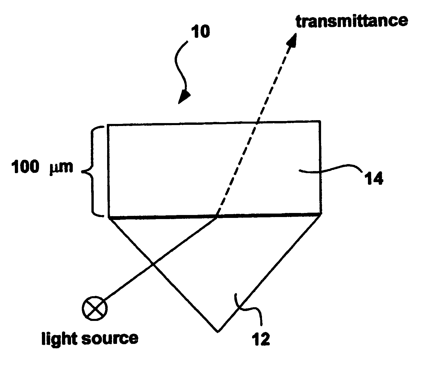
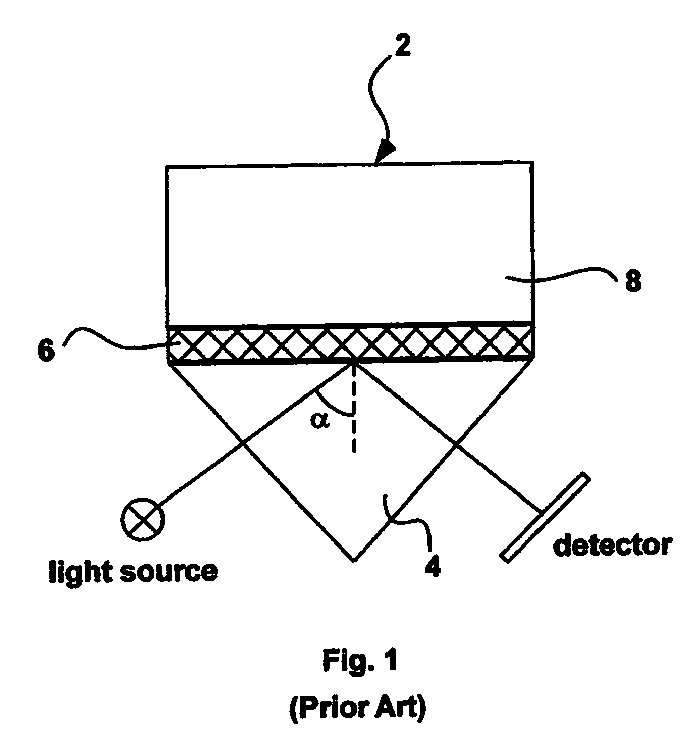
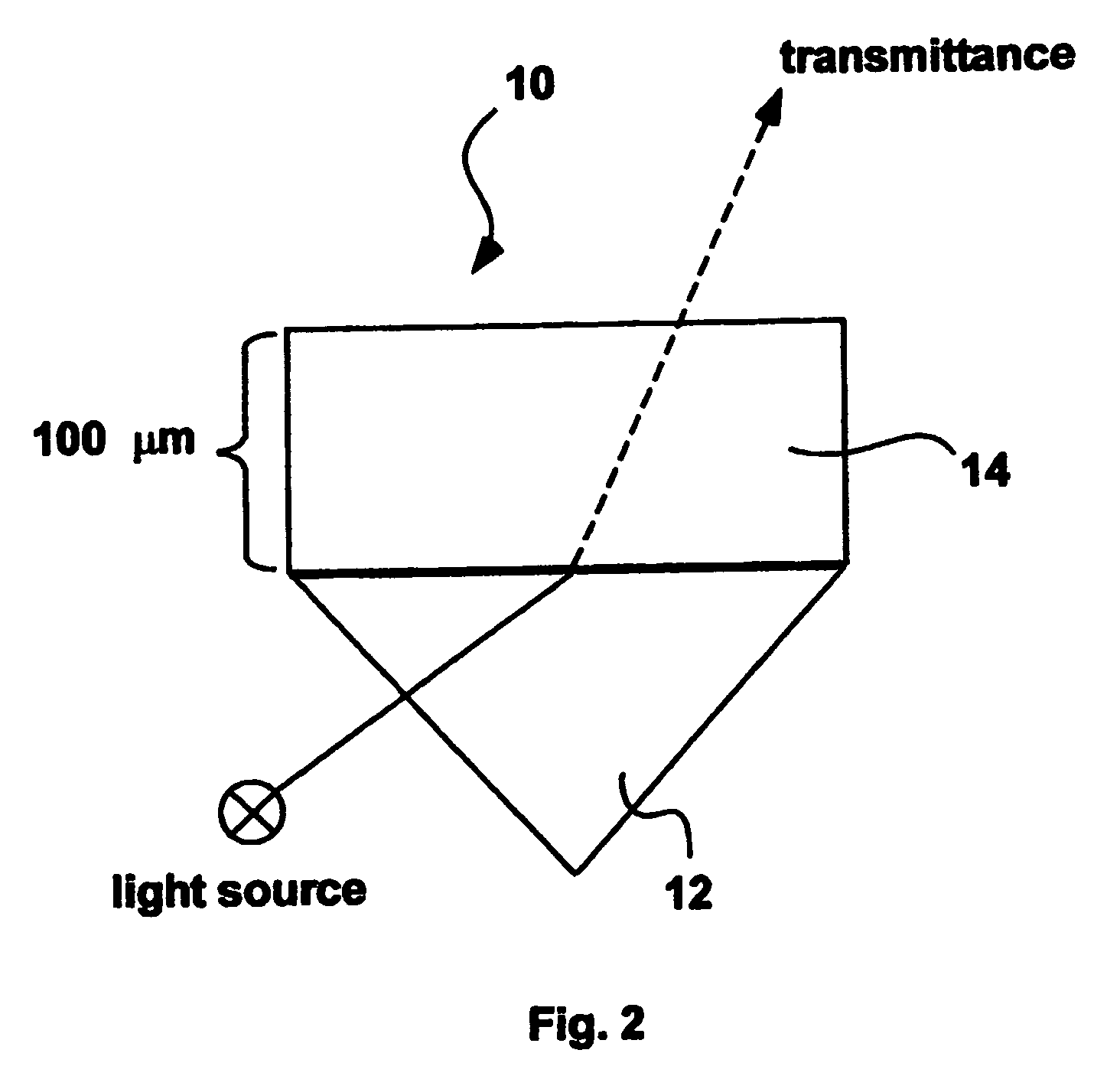
[0045]This invention is the result of further development of the CPWR devices described in our previous U.S. Pat. Nos. 6,421,128; 6,330,387; 5,991,488. In general the invention relates to a sensor for measuring the properties of molecules at surfaces and interfaces that has a dielectric layer or member that is of an optical thickness selected to produce an observable interference effect for an incident angle of light below a critical angle of total internal reflection. Moreover, the invention involves a sensor that combines the phenomena of optical interference and coupling of plasmons into waveguide modes in one sensing device. Thus, the sensor of the invention may be used to measure observable effects that occur both above and below the critical angle for total internal reflection.

[0046]It should be understood that the dielectric layer of the invention is in addition to and separate from the sample material or analyte with which the invention is used. The sample material at the in...


PUM

PropertyMeasurementUnit
thicknessaaaaaaaaaa
thicknessaaaaaaaaaa
incident angleaaaaaaaaaa

Abstract

Methods for measuring a property of a sample material present at an interface of an emerging medium in a spectroscopic device include a sensor (10) featuring at least one dielectric member (14) disposed upon a entrant medium (12), with the dielectric member being of an optical thickness selected to produce an observable interference effect for an incident angle of light below the critical angle of total internal reflection at the interface with the dielectric member (14). The dielectric member (14) of the sensor device (10) may be modified and functionalized for binding of a sample analyte by disposing a sensing surface area (38, 40, 42) upon it. Moreover, an metal layer (18) may be added to an entrant medium (20) to produce a sensor (16) that generates observable optical phenomena both above (resonance) and below (interference) a given critical angle.

Description

U.S. GOVERNMENT RIGHTS[0001]This invention was made with Federal Government support under Contract Number MCB-9904753 awarded by the National Science Foundation and Contract Number GM-59630 awarded by the National Institutes of Health. The Government has certain rights in the invention.CROSS-REFERENCE TO RELATED APPLICATIONS[0002]This application claims benefit of priority under 35 U.S.C. 119(e) to International Application No. PCT / US03 / 30694 filed on Sep. 30, 2003, the entire contents of which are incorporated herein by reference.BACKGROUND OF THE INVENTION[0003]1. Field of the Invention[0004]This invention relates in general to optical sensor chips and more particularly to an optical sensor chip that utilizes the phenomenon of optical interference to spectroscopically characterize the properties of molecules below the critical angle of incidence.[0005]2. Description of the Related Art[0006]Surface plasmon resonance is a phenomenon used in many analytical applications in metallurgy...

Claims


Application Information

Patent Timeline
Patent Type & Authority Patents(United States)
IPC IPC(8): G01N21/55
CPCG01N21/553
Inventor SALAMON, ZDZISLAWTOLLIN, GORDON
Owner THE ARIZONA BOARD OF REGENTS ON BEHALF OF THE UNIV OF ARIZONA
Why Eureka
Try Eureka