MEMS pixel sensor

a micro-electromechanical and sensor array technology, applied in the direction of force measurement using piezo-resistive materials, acceleration measurement using interia forces, instruments, etc., can solve the problems of large impact, noise inherent in the electrical connection between the mems package and the rest of the system, and large proportion of the total cost of the mems devi

Inactive Publication Date: 2008-09-16
SHARP KK
View PDF10 Cites 100 Cited by
  • Summary
  • Abstract
  • Description
  • Claims
  • Application Information

AI Technical Summary

Problems solved by technology

One problem with this type of MEMS packaging methodology is that the package is a very large proportion of the total MEMS device cost; on the order of 30- 70% of the overall cost.
This packaging cost can, therefore, have a significant impact on the capability of such MEMS devices to penetrate cost-sensitive markets, such as the cell phone market.
Another problem with existing MEMS packaging is the noise inherent with the electrical connections between the MEMS package and the rest of the system.
The bonding, wiring, and electrical interconnections associated with interfacing a MEMS device embedded in a package, to a circuit, necessarily adds impedance mismatches that result in noisy or low amplitude signals.
The issues preventing MEMS penetration into the cell phone market are cost and performance.
This cost issue is preventing the integration of MEMS into cell phones, display systems, and many other types of electronic devices.
The integration of MEMS into larger scale systems has been expensive to fabricate due to the process difficulties and the cost associated with integrating the MEMS standard IC technologies, such as CMOS.
The crystallization procedures are also limited by the temperature sensitivity of the substrate material.
MEMS structures are varied and, therefore, more difficult to standardize, as compared to the above-mentioned thin film processes.
Many of the MEMS devices that have been fabricated to date have more theoretical than practical application, as the devices are often difficult and expensive to make.
For the same reason, larger scale systems using MEMS components, have been expensive to fabricate due to the process difficulties and the cost associated with integrating the MEMS and IC technologies.
For example, transistors and associated MEMS structures have been fabricated on bulk Si substrates, However, the etching processes needed to form a bulk silicon MEMS -are more difficult to control, dramatically limit available process steps, and require long etch times. These limitations make these devices unsuitable for low-cost integrated systems.
However, these sensing schemes cannot be applied to low temperature TFT process, because the changes in electrical characteristics induced as a result of stress change are too small to be practically measured.
1) High cost: current microarray technology is very expensive with the most expensive being the Affymetrix-type. The “genechip” is a single use device that costs on the order of $300 to $500 per chip. In addition, several pieces of additional process equipment are required: among them a washing station and scanner. The process requires the scanning of the “genechip” (with the material of interest applied to the chip) with a laser, florescent material on the chip is activated and a light imager records the image of the florescent pattern. Then, the result must be interpreted using templates to analyze the image.
2) Low throughput: While current microarray technology has produced a very high volume of data for genetic research, the process is still relatively slow. For example, a DNA hybridization experimental process takes a minimum of several hours and more likely overnight to complete.
3) Inaccuracies: The current DNA microarray technology produces results with inaccuracies such as false positives.
4) Bulky system: The current microarray technology requires an assortment of process equipment. In addition to the equipment required to prepare the array, a laser scanner and image detection system are required to read the result. Thus, this technology cannot produce a portable solution for microarray applications.

Method used


Image

  • MEMS pixel sensor
  • MEMS pixel sensor
  • MEMS pixel sensor

Examples


Embodiment Construction

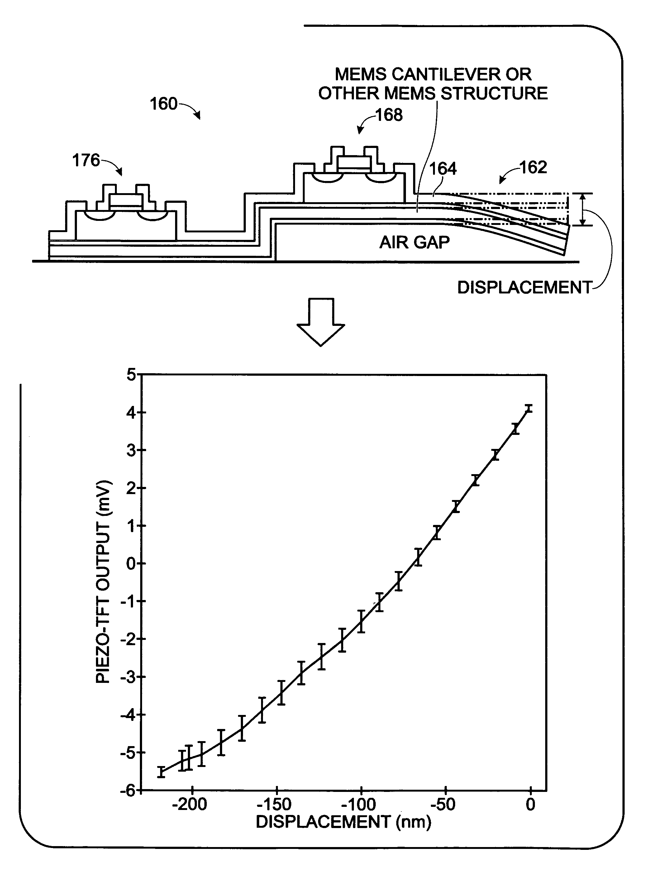
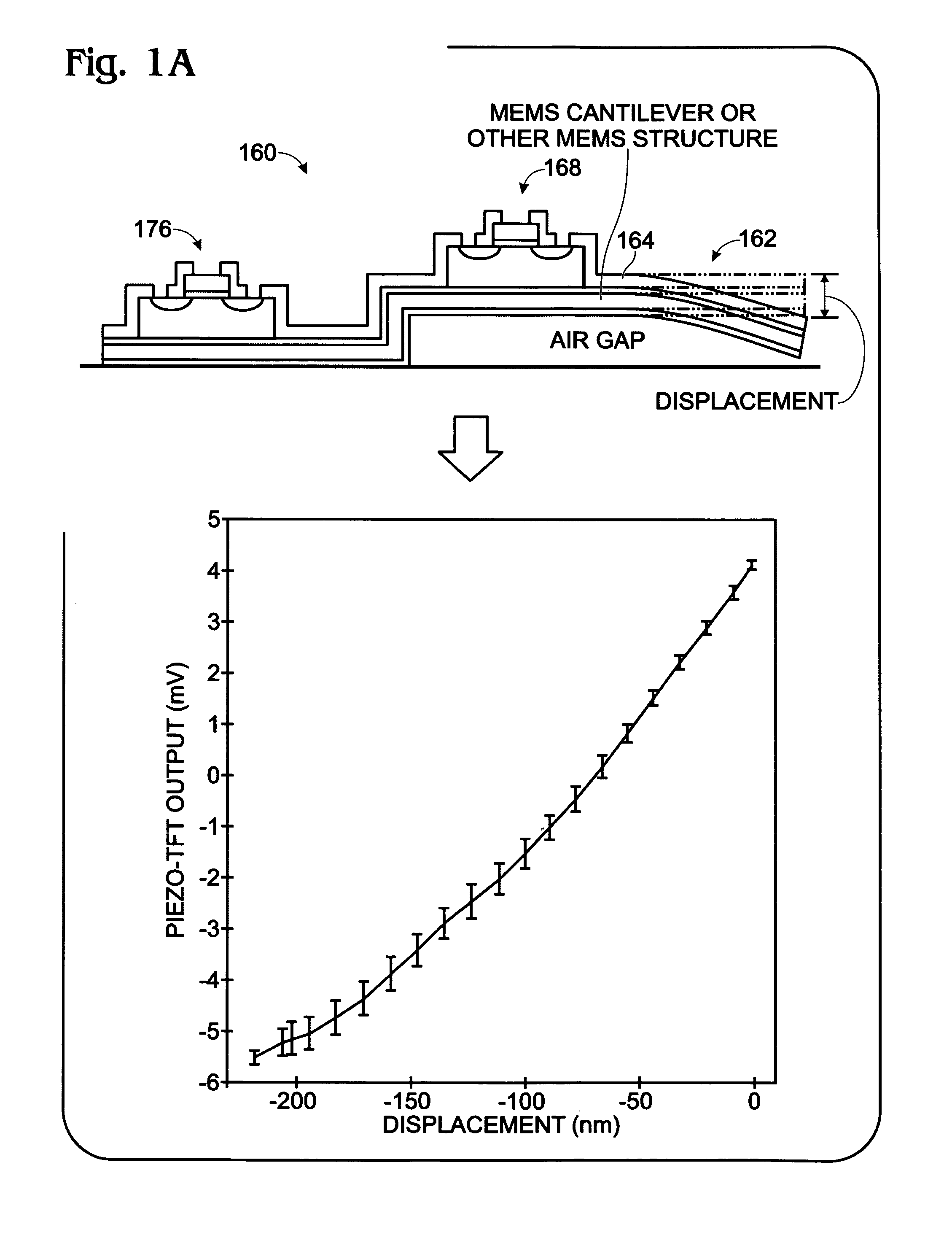
[0071]FIGS. 1A through 1H depict various aspects of a MEMS pixel sensor and associated array. The present invention MEMS pixel sensor provides a fabrication process, device design, and an integrated sensor array system that displays improvements in the area of cost, speed, compactness, and accuracy with respect to conventional technology. In the following discussion a piezo-TFT cantilever is often presented as an example of a MEMS pixel sensor. In other aspects, the MEMS pixel sensor is described more concisely as a transducer, MEMS, MEMS sensor, pixel, process pixel, or MEMS pixel.

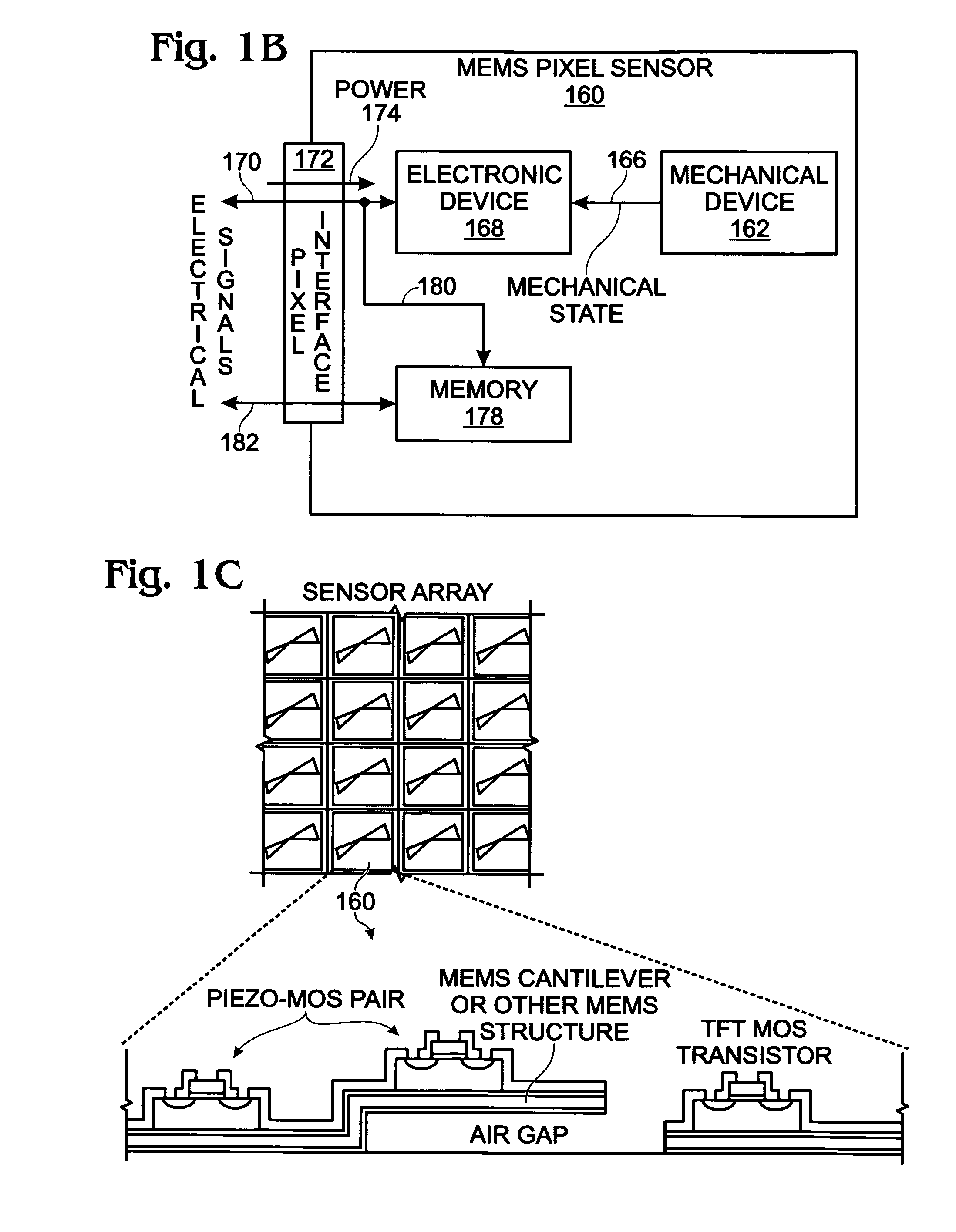
[0072]FIG. 1A is a cross-sectional view of a MEMS pixel sensor (MPS). FIG. 1B is schematic block diagram view of the MEMS pixel sensor of FIG. 1A. FIGS. 1C and 1D show the MPS of FIG. 1A as part of a sensor array.

[0073]1) Fabrication process: Low temp poly processing including laser anneal enables the monolithic fabrication of a single transducer that includes both electrical and mechanical elements that ...


PUM

PropertyMeasurementUnit
thickaaaaaaaaaa
thickaaaaaaaaaa
output voltagesaaaaaaaaaa

Abstract

A MEMS pixel sensor is provided with a thin-film mechanical device having a mechanical body, with a mechanical state responsive to a proximate environment. A thin-film electronic device converts the mechanical state into electrical signals. A pixel interface supplies power to the electronic device and transceives electrical signals. The sensor is able to operate dynamically, in real-time. For example, if the mechanical device undergoes a sequence of mechanical states at a corresponding plurality of times, the electronic device is able to supply a sequence of electrical signals to the pixel interface that are responsive to the sequence of mechanical states, at the plurality of times. Each MEMS pixel sensor may include a number of mechanical devices, and corresponding electronic devices, to provide redundancy or to measure a broadband response range.

Description

RELATED APPLICATIONS[0001]This application claims priority, under 35 U.S.C. 119, to Provisional Application No. 60 / 720,223, entitled BIOCHEMICAL MEMS SENSOR, filed Sep. 23, 2005, and assigned to the assignee hereof.[0002]This application is a continuation-in-part of a patent application entitled, MICROELECTROMECHANICAL THIN-FILM DEVICE, invented by John Hartzell, Ser. No. 11 / 058,501, filed Feb. 14, 2005, now U.S. Pat. No. 7,230,306, which is a continuation of Ser. No. 10 / 131,057, filed Apr. 23, 2002, issued as U.S. Pat. No. 6,860,939.[0003]This application is a continuation-in-part of a patent application entitled, PIEZO-TFT CANTILEVER MEMS, invented by Zhan et al., Ser. No. 11 / 031,320, filed Jan. 5, 2005, now U.S. Pat. No. 7,253,488.[0004]This application is a continuation-in-part of a patent application entitled, CRYSTAL-STRUCTURE-PROCESSED MECHANICAL DEVICES AND METHODS AND SYSTEMS FOR MAKING, invented by John Hartzell, Ser. No. 10 / 131,318, filed Apr. 23, 2002, now U.S. Pat. No. ...

Claims


Application Information

Patent Timeline
Patent Type & Authority Patents(United States)
IPC IPC(8): H01L29/66G01N27/00
CPCB81C1/00246G01L1/16G01L1/18H04R17/02H04R31/00H01L27/20H01L27/12H04R2499/11H04R19/00H10N39/00
Inventor HARTZELL, JOHN WALTERZHAN, CHANGQINGWOLFSON, MICHAEL BARRETT
Owner SHARP KK
Why Eureka
Try Eureka