Method for fabricating isolation structures for flash memory semiconductor devices

a technology of isolation structure and memory device, which is applied in the direction of semiconductor devices, basic electric elements, electrical equipment, etc., can solve the problems of reducing the efficiency and reducing the cost of integrated circuit or chip fabrication. , to achieve the effect of improving process integration, facilitating use, and increasing the yield of dies per wafer

Active Publication Date: 2008-09-23
SEMICON MFG INT (SHANGHAI) CORP
View PDF4 Cites 47 Cited by
  • Summary
  • Abstract
  • Description
  • Claims
  • Application Information

AI Technical Summary

Benefits of technology

[0009]Many benefits are achieved by way of the present invention over conventional techniques. For example, the present technique provides an easy to use process that relies upon conventional technology. In some embodiments, the method provides higher device yields in dies per wafer. Additionally, the method provides a process that is compatible with conventional process technology without substantial modifications to conventional equipment and processes. Preferably, the invention provides for an improved process integration for design rules of 90 nanometers and less for high density Flash devices. In a preferred embodiment, we are able to form dual STI trench depth with no additional reticle or masking steps required for a Flash memory process. This method will gain advantages of having shallower trench depth in cell array at minimum cost. Depending upon the embodiment, one or more of these benefits may be achieved. These and other benefits will be described in more throughout the present specification and more particularly below.

Problems solved by technology

An integrated circuit or chip fabrication facility can cost hundreds of millions, or even billions, of U.S. dollars.
Making devices smaller is very challenging, as each process used in integrated fabrication has a limit.
Additionally, as devices require faster and faster designs, process limitations exist with certain conventional processes and materials.
Although there have been significant improvements, such device designs still have many limitations.
As merely an example, these designs must become smaller and smaller but still provide clear signals for switching, which become more difficult as the device becomes smaller.
Additionally, these designs are often difficult to manufacture and generally require complex manufacturing processes and structures.

Method used


Image

  • Method for fabricating isolation structures for flash memory semiconductor devices
  • Method for fabricating isolation structures for flash memory semiconductor devices
  • Method for fabricating isolation structures for flash memory semiconductor devices

Examples


Embodiment Construction

[0013]According to the present invention, techniques for processing integrated circuits for the manufacture of semiconductor devices are provided. More particularly, the invention provides a method and structure for manufacturing isolation structures for memory devices. Merely by way of example, the invention has been applied to the manufacture of Flash memory devices. But it would be recognized that the invention has a much broader range of applicability.

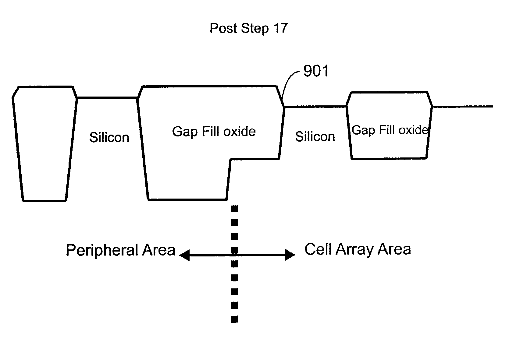
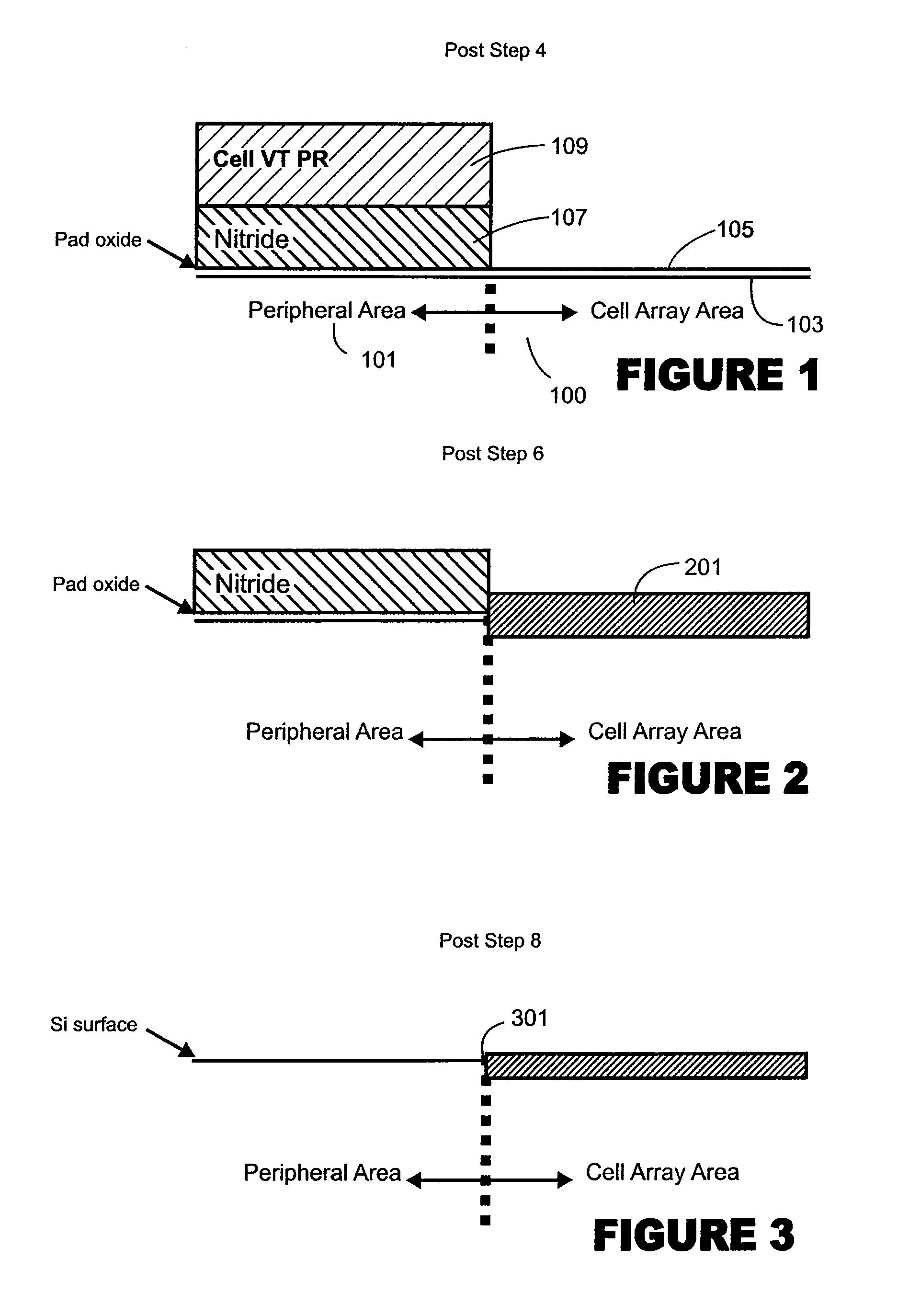
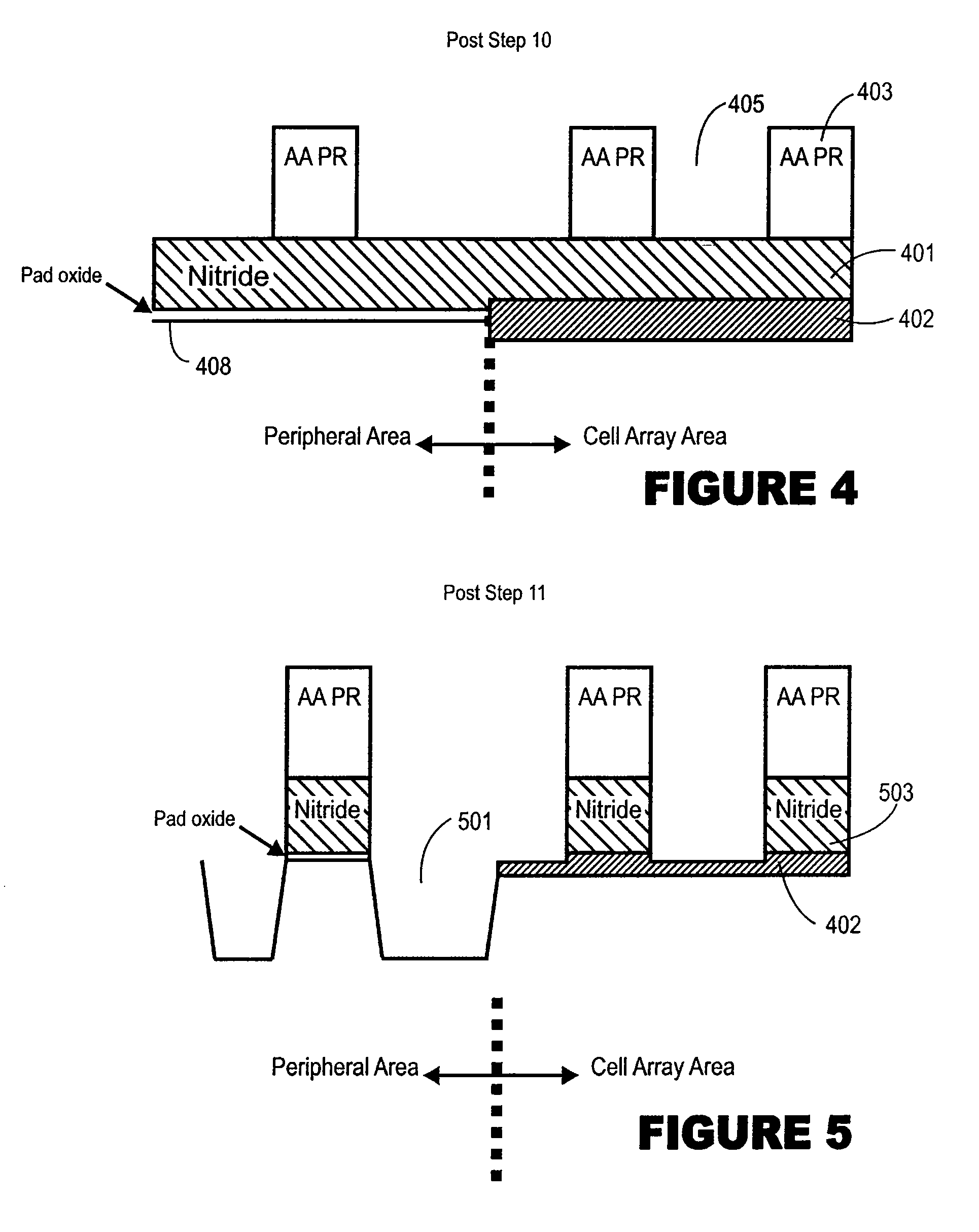
[0014]Self aligned source (SAS) is widely used in ETOX type Flash Memory processes in order to reduce the cell size along bit-line direction. At the same time, it is often required to have low source line resistance in order to minimize the unwanted voltage drops along the source line. Isolation pitch, trench depth and source junction profiles are the key factors to determine the source line resistance. As process feature shrinks, deeper trench (˜3500 Angstroms) is widely adopted in standard logic processes in order to meet the str...


PUM

PropertyMeasurementUnit
depthaaaaaaaaaa
depthaaaaaaaaaa
thicknessaaaaaaaaaa

Abstract

A method for fabricating integrated circuit devices, e.g., Flash memory devices, embedded Flash memory devices. The method includes providing a semiconductor substrate, e.g., silicon, silicon on insulator, epitaxial silicon. In a specific embodiment, the semiconductor substrate has a peripheral region and a cell region. The method includes forming a first dielectric layer (e.g., silicon dioxide) having a first thickness overlying a cell region and a second dielectric layer (e.g., silicon dixode) having a second thickness overlying the peripheral region. In a specific embodiment, the cell region is for Flash memory devices and / or other like structures. The method forms a pad oxide layer overlying the first dielectric layer and forms a nitride layer overlying the pad oxide layer. The method includes patterning at least the nitride layer to expose a first trench region in the peripheral region and to expose a second trench region in the cell region, while a portion of the first dielectric layer having the first thickness in the cell region is maintained. The method includes forming a first trench structure having a first depth in the first trench region, while the portion of the first dielectric layer having the first thickness in the cell region protects the second trench region. The method includes removing the portion of the first dielectric layer to expose the second trench region. In a specific embodiment, the method includes subjecting the first trench region, including the first trench structure, and the second trench region with an etching process to continue to form the first trench structure from the first depth to a second depth and to form a second trench structure having a third depth within the second trench region. In the third depth is less than the second depth.

Description

CROSS-REFERENCES TO RELATED APPLICATIONS[0001]This application claims priority to Chinese Application No. 200510111386.4; filed on Dec. 5, 2005; commonly assigned, and of which is hereby incorporated by reference for all purposes.BACKGROUND OF THE INVENTION[0002]The present invention is directed to integrated circuits and their processing for the manufacture of semiconductor devices. More particularly, the invention provides a method and structure for manufacturing isolation structures for memory devices. Merely by way of example, the invention has been applied to the manufacture of Flash memory devices. But it would be recognized that the invention has a much broader range of applicability.[0003]Integrated circuits have evolved from a handful of interconnected devices fabricated on a single chip of silicon to millions of devices. Conventional integrated circuits provide performance and complexity far beyond what was originally imagined. In order to achieve improvements in complexit...

Claims


Application Information

Patent Timeline
Patent Type & Authority Patents(United States)
IPC IPC(8): H01L21/76
CPCH01L27/11521H01L27/115H01L21/76232H01L21/76229H10B69/00H10B41/30
Inventor JIN, DATANG, SHU SHUYANG, ZUO YA
Owner SEMICON MFG INT (SHANGHAI) CORP
Why Eureka
Try Eureka