Semiconductor light emitting device substrate and method of fabricating the same

a technology of light emitting device and substrate, which is applied in the direction of semiconductor devices, basic electric elements, electrical equipment, etc., can solve the problems of increasing resistance, increasing density at the etched portions, and affecting the electrical properties of light emitting diodes, so as to achieve the effect of higher light emitting efficiency

Inactive Publication Date: 2008-09-23
IND TECH RES INST
View PDF10 Cites 27 Cited by
  • Summary
  • Abstract
  • Description
  • Claims
  • Application Information

AI Technical Summary

Benefits of technology

[0011]The present invention is related to a semiconductor light emitting device substrate, so as to obtain higher light emitting efficiency by the use of the semiconductor light emitting device grown on the substrate.
[0012]Moreover, the present invention is related to a semiconductor light emitting device substrate, so as to obtain higher output power by the use of the semiconductor light emitting device grown on the substrate.
[0013]Furthermore, the present invention is related to a method of fabricating a semiconductor light emitting device substrate, which can decrease the defect and stress of the semiconductor light emitting device grown on the substrate.
[0017]Because to the periodic nanocrystal structure is disposed on the surface of the substrate, the present invention has the following advantages. (1) The semiconductor material grown on the substrate has fewer defects. (2) The semiconductor light emitting device grown on the substrate has higher light emitting efficiency. (3) The semiconductor light emitting device grown on the substrate has higher optical output power. (4) The material stress of the semiconductor light emitting device grown on the substrate is reduced.

Problems solved by technology

However, the pattern 104a (i.e., the nanocrystal structure) of the P-type GaN layer 104 is usually fabricated in manner of etching, such that the defect density at the etched portions increases, leading to the increase of resistance, thus influencing the electrical property of the light emitting diode.

Method used


Image

  • Semiconductor light emitting device substrate and method of fabricating the same
  • Semiconductor light emitting device substrate and method of fabricating the same
  • Semiconductor light emitting device substrate and method of fabricating the same

Examples


first embodiment

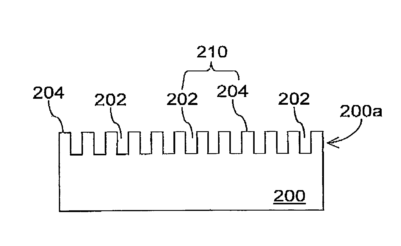
[0026]FIG. 2 is a schematic sectional view of the semiconductor light emitting device substrate according to the present invention.

[0027]Referring to FIG. 2, the semiconductor light emitting device substrate 200 of the first embodiment has a nanocrystal structure 210, which is a periodic structure. The nanocrystal structure 210 is disposed on a surface 200a portion of the substrate 200, and has an etched region 202 and an unetched region 204. The material of the substrate 200 is a single crystal material, for example, transmissive and does not absorb in wavelength range of visible light and infrared light. The single crystal material is, for example, Al2O3 (sapphire), LiAlO2, LiGaO2, SiC, GaN, AlN, AlGaN, or another suitable single crystal material.

[0028]Referring to FIG. 2 again, the step of forming the nanocrystal structure 210 includes defining a pattern on the surface 200a of the single crystal material with a lithographic process, which is a pattern such as a network, columnar,...

second embodiment

[0035]FIG. 8 is a schematic sectional view of a semiconductor light emitting device substrate according to the present invention.

[0036]Referring to FIG. 8, the second embodiment is similar to the first embodiment, and only the difference is described below. In addition to a single crystal material 801 having a nanocrystal structure 810, the substrate 800 of the second embodiment further includes an undoped nitride semiconductor layer 806 on the surface of the single crystal material 801. The single crystal material 801 and the undoped nitride semiconductor layer 806 form a substrate, and the nanocrystal structure 810 also has an etched region 802 and an unetched region 804. The material of the substrate is, for example, transmissive and does not absorb in wavelength range of visible light and infrared light. The undoped nitride semiconductor layer 806 is, for example, a nitride semiconductor material containing at least one of In, Al, or Ga, such as GaN, AlN, InN, AlGaN, InGaN, AlIn...


PUM


Abstract

A substrate for semiconductor light emitting devices is provided. The substrate is characterized in that the substrate is a single crystal material and has a nanocrystal structure capable of diffracting an electromagnetic wave. The nanocrystal structure is disposed on a surface portion of the substrate and includes an etched region and an unetched region, wherein the etched region has a depth of 10-200 nm. Due to the periodicity of the nanocrystal structure, the semiconductor material grown on the substrate has fewer defects, and the material stress is reduced.

Description

CROSS-REFERENCE TO RELATED APPLICATION[0001]This application claims the priority benefit of Taiwan application serial no. 95121557, filed Jun. 16, 2006. All disclosure of the Taiwan application is incorporated herein by reference.BACKGROUND OF THE INVENTION[0002]1. Field of the Invention[0003]The present invention relates to a semiconductor light emitting device structure and a method of fabricating the same. More particularly, the present invention relates to a semiconductor light emitting device structure having a nanocrystal structure and a method of fabricating the same.[0004]2. Description of Related Art[0005]Distinct from the light emitting theory of regular fluorescent lamps or incandescent lamps generating heat to emit light, semiconductor light emitting devices such as light emitting diodes takes advantage of the specific property of semiconductor to emit light, and thus the light emitted by light emitting diodes is referred to as cold luminescence. The light emitting diode...

Claims


Application Information

Patent Timeline
Patent Type & Authority Patents(United States)
IPC IPC(8): H01L29/06H01L21/00H01L29/26H01L33/00H01L33/12H01L33/16H01L33/20
CPCH01L33/20H01L33/16H01L33/007H01L33/12H01L2933/0083H01L33/382
Inventor CHUO, CHANG-CHENGLAI, CHIH-MING
Owner IND TECH RES INST
Why Eureka
Try Eureka